Nvidia reveals Volta GV100 GPU and the Tesla V100
A new architecture and Tensor cores, all designed for machine learning.
Nvidia's yearly GPU Technology Conference is going on this week in San Francisco, and unlike Intel's IDF, which was recently given the axe in favor of smaller, focused product launches, GTC is alive and well. With more attendees and presentations, one might think GPUs are outpacing the growth of other processors, and Nvidia readily agrees. And much like last year's event, the focus is clearly on machine learning and AI.
Sorry to say, but I have no Terminator and SkyNet references for you. Instead, I've got specs for the first of Nvidia's next-generation Volta architecture GPUs. If you were underwhelmed with Pascal and basically felt it was Maxwell at 16nm FinFET, with a few minor tweaks, Volta is a very different beast.
Similar to last year's GP100 announcement, Volta is starting at the very top of the product stack with a massive GV100 chip that may never find its way into a consumer product. And that's fine, because variations of Volta are still on track, and based on the timing of the GV100 launch, they may come sooner rather than later.
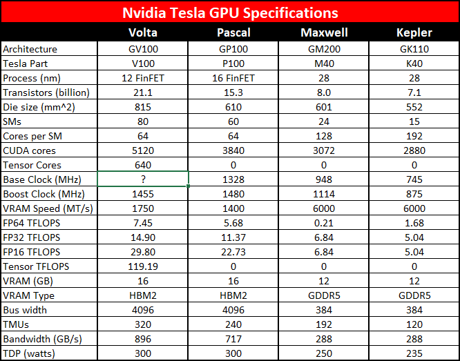
Keep in mind the positioning of GV100 as a compute and machine learning focused product as I continue into the specs, because the consumer parts will probably omit some of the new features. For now, GV100 takes the crown for the largest chip Nvidia—or anyone else—has ever created, and by a wide margin! Check out the specs:

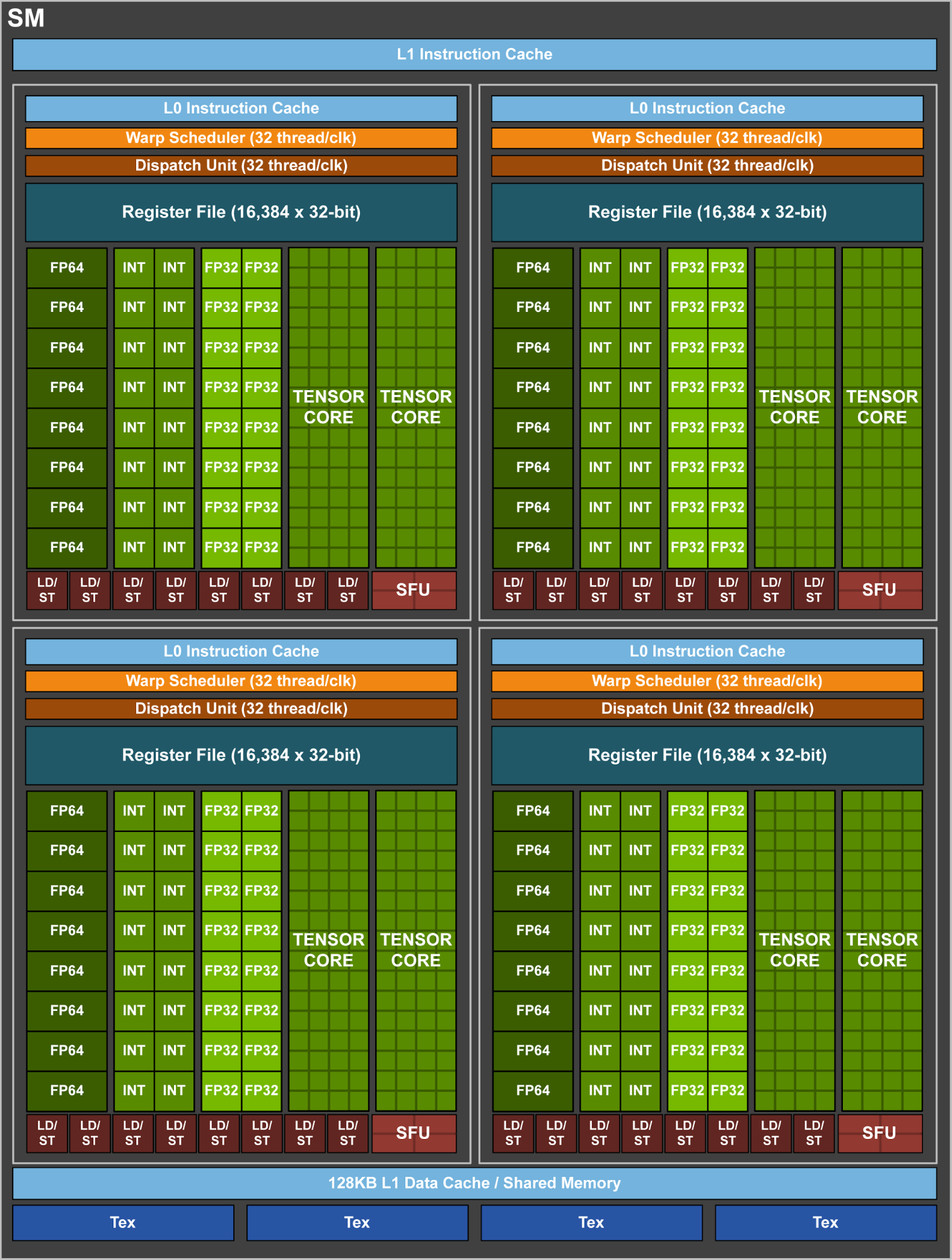
There are a few key items to point out with the new Volta GPU. First, unlike previous Nvidia GPUs, there's a new core type, what Nvidia calls a Tensor Core. This is in addition to CUDA cores and is a more densely packed but slightly less flexible core, which works on data in 4x4 matrices. Each Tensor core can do a fused multiply add (FMA) operation on 4x4 matrices (A * B + C), which represents 128 floating-point operations (FLOPS).
With eight Tensor cores per SM, that works out to 1024 FLOPS per clock per SM, and in the case of the Tesla V100 that's 81,920 FLOPS per clock. With a peak clockspeed of 1455MHz, that works out to nearly 120 TFLOPS—at least for use cases that can utilize the Tensor cores. As an example of what that means, Nvidia stated that on ResNet-50 training (a deep neural network), the V100 is 2.4 times faster than the P100, and for ResNet-50 inference, it's 3.7 times faster.

The other major item to point out is that the Telsa V100 doesn't use a fully enabled GV100—four SMs are disabled. So potentially there are another 256 CUDA cores and 32 Tensor cores disabled. Given the massive size of the chip, that's not too surprising, and we never saw a fully enabled GP100 product either.
The biggest gaming news, reviews and hardware deals
Keep up to date with the most important stories and the best deals, as picked by the PC Gamer team.
Okay, seriously: 815 mm^2!? GP100 was already huge, and only the IBM POWER8 and Intel Itanium (Tukwila) were slightly larger. GV100 leaves everything else far behind. Part of that size is for the silicon interposer that HBM2 requires, but even so GV100 is ginormous. The 80 active SMs is a 33 percent increase over the GP100, and while the chip is also 33 percent larger, that size increase includes the added Tensor cores plus additional architectural enhancements.
And what might those architectural enhancements be? Nvidia hasn't gone into full disclosure yet, but it has reworked the core layout, memory controllers, thread scheduling and execution, and other aspects of the design—in other words, just about everything has been tweaked in some fashion.
What does all of this mean for Volta-derived GPUs for gaming purposes? With a process shrink to 12nm from 16nm (basically a refinement to TSMC's existing manufacturing process), Nvidia should be able to add more cores to Volta GPUs, and each of those cores will presumably be more efficient than the existing Pascal cores. Volta was originally on the roadmap for a 2018 launch window, but with GV100 now revealed, speculation that consumer Volta cards (GeForce 11-series most likely) will come out later in 2017 seems quite likely. HBM2 remains expensive, however, and GDDR6 or GDDR5X should continue to offer better value.
If you were hoping for a lull in the GPU wars, so that you could sit back and enjoy your shiny new GeForce 1080 Ti as the fastest consumer graphics card around… don't be surprised if a GTX 1180 comes out later this year with a lower price and better performance. My crystal ball is guessing fall right now.
Jarred's love of computers dates back to the dark ages when his dad brought home a DOS 2.3 PC and he left his C-64 behind. He eventually built his first custom PC in 1990 with a 286 12MHz, only to discover it was already woefully outdated when Wing Commander was released a few months later. He holds a BS in Computer Science from Brigham Young University and has been working as a tech journalist since 2004, writing for AnandTech, Maximum PC, and PC Gamer. From the first S3 Virge '3D decelerators' to today's GPUs, Jarred keeps up with all the latest graphics trends and is the one to ask about game performance.


