Journey to the Center of the CPU: 15 Gorgeous Closeups of Microprocessors
Mmm…chips. So darned tasty, such a perfect accompaniment to a frosty glass of beer on a hot summer afternoon. But do any of us really need to see a microscopic view of what goes on inside those yummy spud slabs? Hell no! Most of us are too terrified to even read the list of ingredients.
Computer chips, on the other hand, are ripe for a little up close and personal examination. Particularly the one chip that towers above all others—the big, bad CPU. We know there are millions, and often billions, of transistors packed inside each and every modern-day processor. This in itself is a testament not only to man's obsession with miniaturization but his unstoppable thirst for power. But there's other stuff too—silicon wafers; dielectric insulators; copper electroplating; a high-speed, multi-layered highway of interconnections; and assorted unit-specific bits and pieces.
Wanna see what it all looks like? Check out the gallery below!
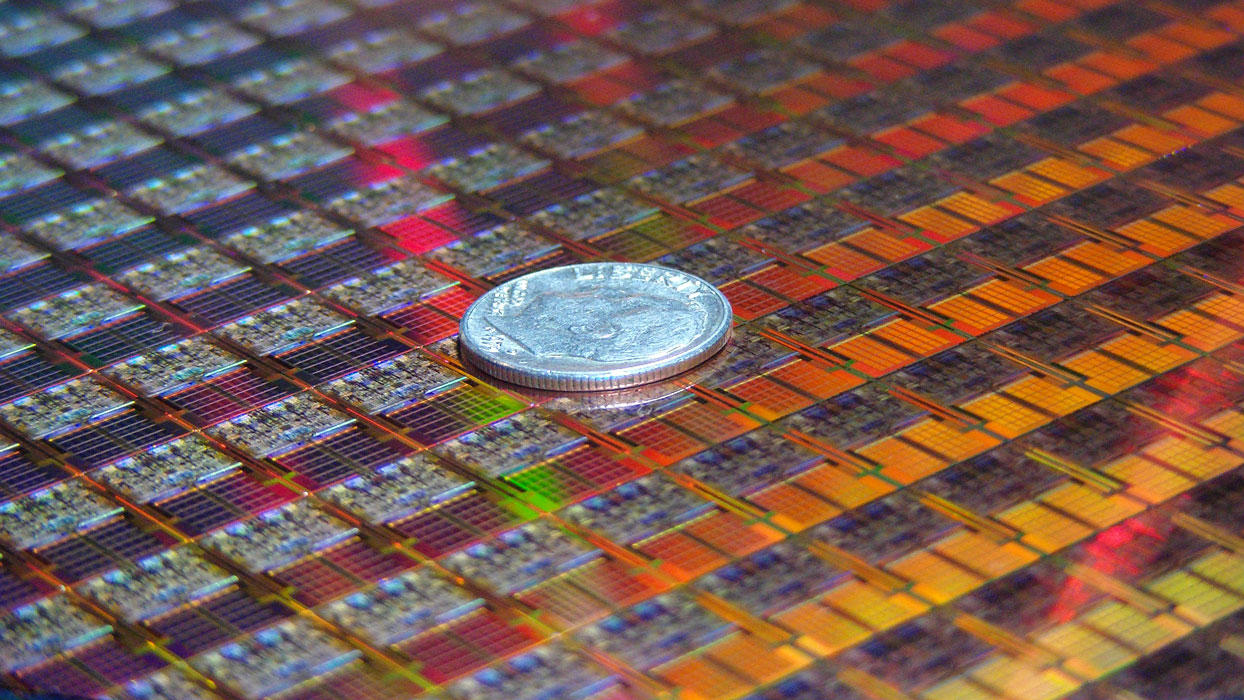
Notable as the first CPU to utilize Intel's 45nm production process, the "Penryn" eventually found its way into a ton of desktops and laptops under the Core 2 and Xeon monikers, delivering faster performance, less heat, and increased efficiency over earlier 65nm processors. Here, we see a Penryn wafer posing coyly with an American dime.
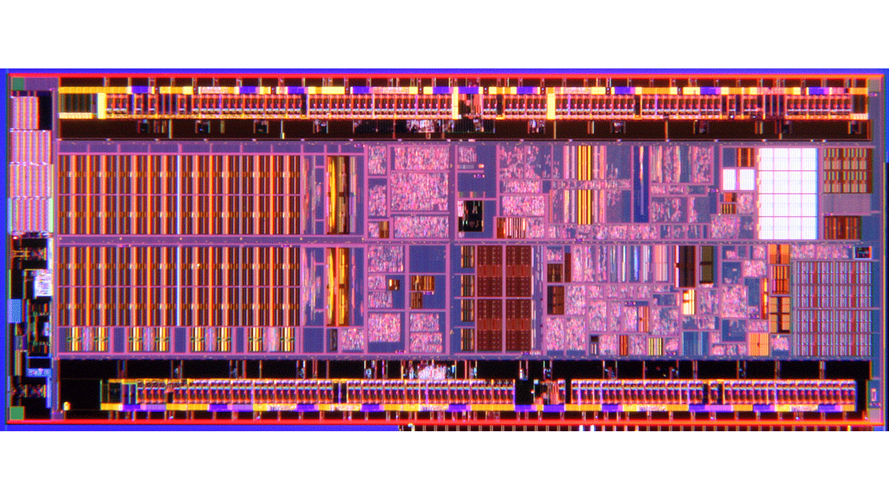
Unveiled in 2009, the processor known as Silverthorne was a comparative lightweight when it came to transistor hording. With "only" 47 million of them, it was no competition for the big boys of the time. However, it didn't need to be. Smaller than a penny, the new kid in town was aimed squarely at the ultra-mobile market, where it soon gained fame as the "Atom."

Steve Chamberlin was a man on a mission. Back in November 2007, Steve set out to build a homebrew CPU. A roll-your-own computer brain. And not just some trumped-up calculator either. Steve wanted his creation to "be fast enough to run interesting programs interactively." Amazingly, he'd reached his goal by early 2009. You can find more information on the methods behind Steve's madness, but in the meantime, enjoy this shot of a big mess o' wires.
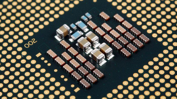
The Intel-AMD cage match to the death has persisted, unabated, since the dawn of the industrial age. Don't believe us? That is your prerogative. But one thing is sure – high-level competition in the processor game is a great thing for consumers. The photo above, for example, may be a close-up of an Intel Core 2 Quad Q8400, but it's also the very affordable physical manifestation of Intel's response to AMD's Phenom II X4 940. Would we have the former without the latter?
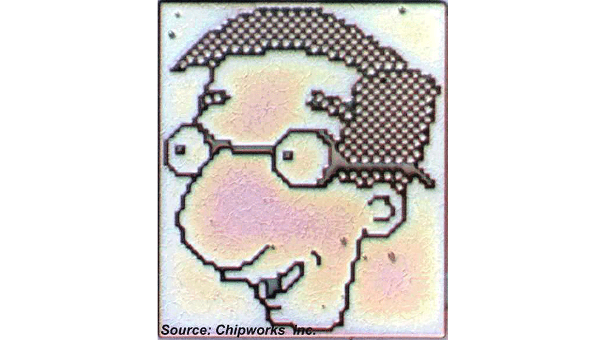
Canadian concern Chipworks likes to dismantle stuff. It especially likes dismantling chips and checking for patent infringements. Or unraveling microscopic mysteries. Yet not all of those mysteries are readily apparent. Sometimes when Chipworks digs really deep, it uncovers surprisingly "human" details. Evidence that yes, engineers really do have a sense of humor. Take this shot of Springfield's fave nerd, for example, found inside the Silicon Image Sil154CT64 digital transmitter.
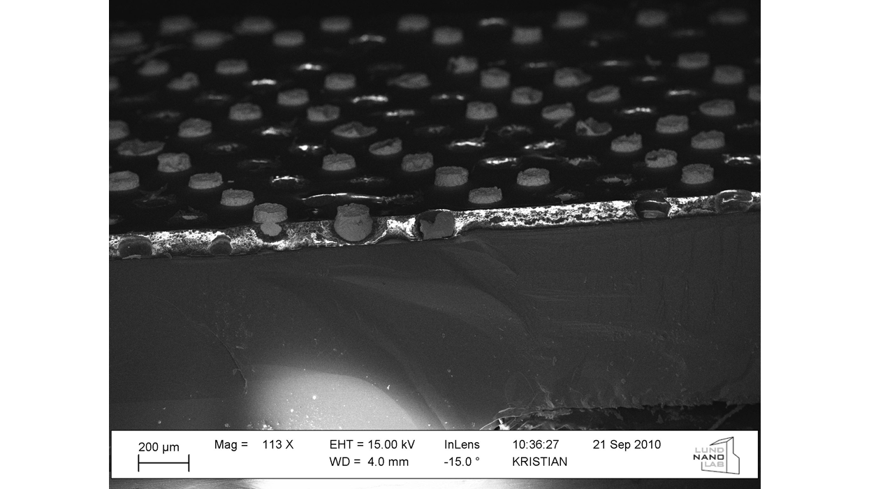
What do you get when you mix a power saw with a pair of pliers and a scalpel? The ingredients for an episode of Criminal Minds? Well, yes, there's that. But you also get the necessary groundwork for a Pentium III autopsy. And that's precisely what's happened over at www.sciencystuff.com, where an industrious PhD student tore open an old school Pentium III processor and put the gaping wounds under an electron microscope. Here we see a view of the edge of his brutally abused PIII chip.
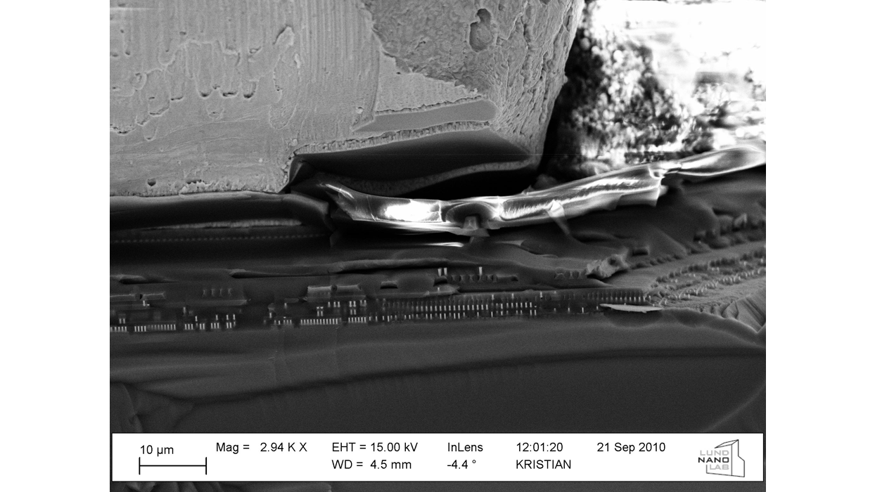
Following up on the previous image, pulled from the oh-so-gruesome Pentium III autopsy at www.sciencystuff.com, we see here an incrementally closer, gorier perspective (3000x magnification) of the same chip edge. Oh the humanity!
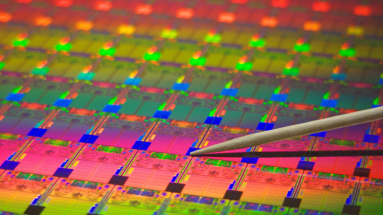
According to developer Intel, the Penryn processor, debuting in 2007 and based on Intel's 45nm Hafnium-based High-k Metal Gate "Penryn" wafer, incorporated 410 million transistors (in dual core configuration), and 820 million of the little buggers (in quad core config). Here, a Penryn uses a normal, everyday toothpick for decorative purposes.
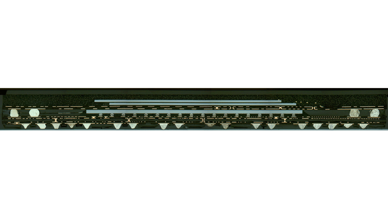
California's iFixit is a homebrew outfit specializing in tearing down electronic gadgets and publishing data describing how they do it. So when iFixit joined up with semiconductor reverse engineering dudes Chipworks to deconstruct an Apple (Samsung) A5 system-on-a-chip, typically found in recent vintage iPads and iPhones, you just knew there had to be photos. Above is a cross-section of the CPU and RAM package. The center rectangle is the processor, the two rectangles above it are RAM dies.
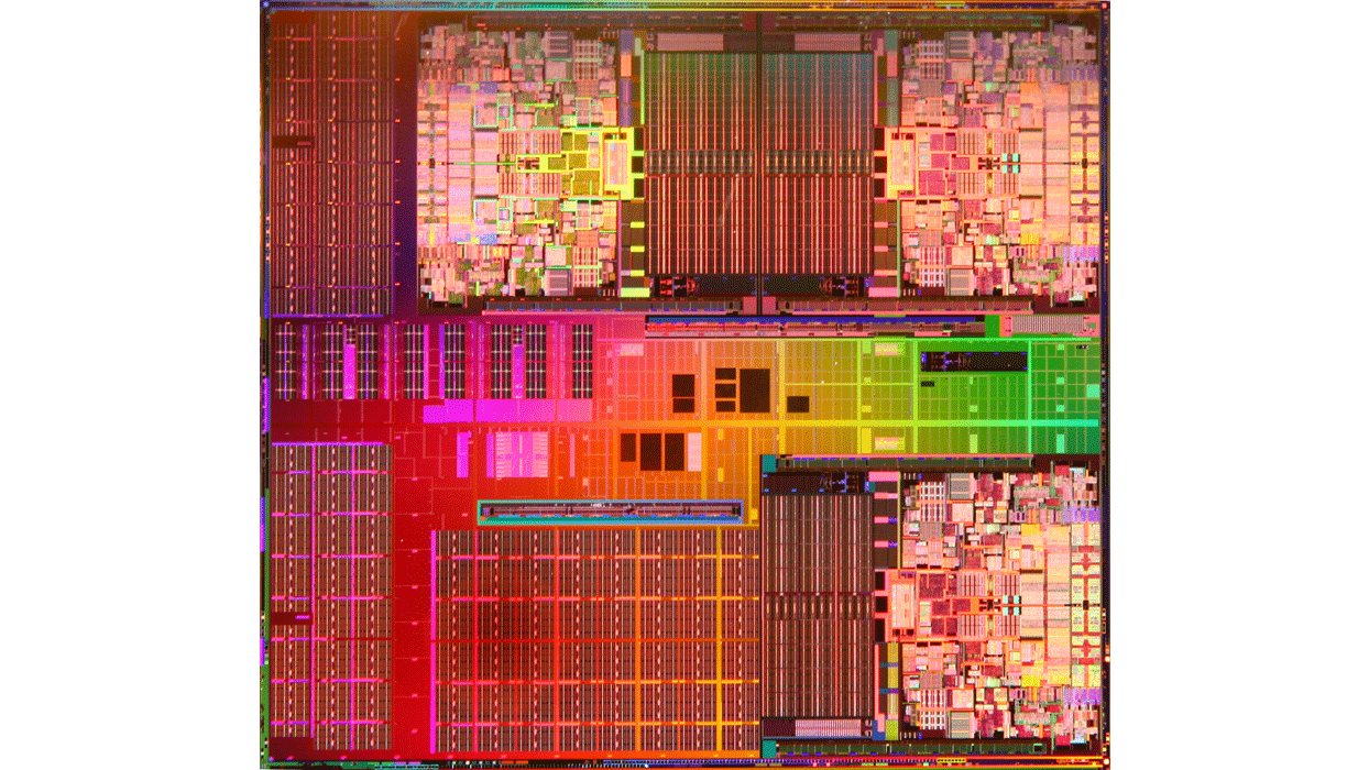
If you think the above shot is color enhanced, well, you might be right. After all, post-processing these days isn't exactly rocket science. Yet those trained in the art of processor photography swear that processors simply look this way when flooded with proper lighting. In any case, enjoy all the colors of the rainbow in this 2008 capture of an Intel Dunnington processor, the first Intel Architecture CPU with six cores.
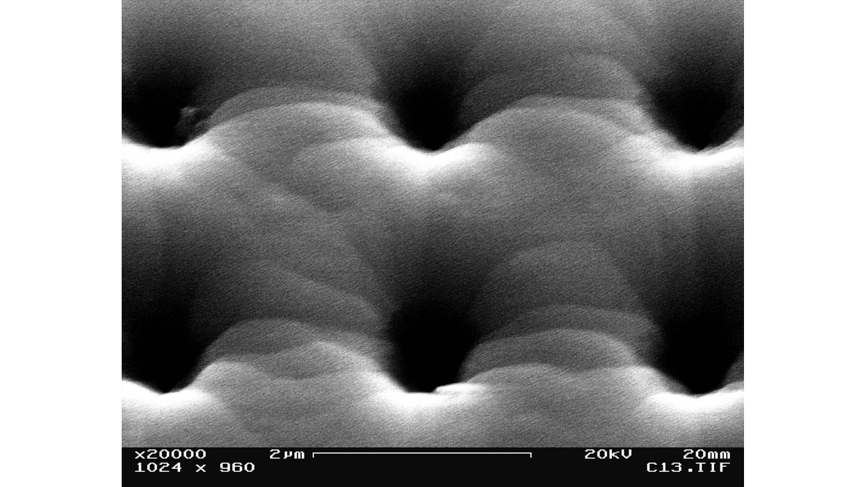
Way back in the middle of the last decade, a fellow by the name of Alex Pisarski at the University of Rochester had a hankering to verify Moore's Law. He took an electron microscope to a 1989 Intel 486 and a 1992 Pentium and created a gaggle of nifty images. This 20,000x magnification of the wire interconnect holes of a 486 is one of them. Check out more Pisarski pics here.
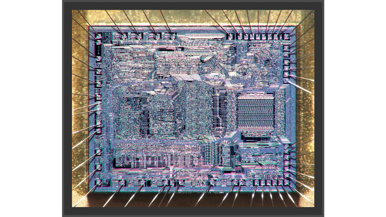
This gleaming top-down look at an extremely antiquated AMD Am2903ADC bit-slice processor is evidence that even decades ago, CPUs were highly complex affairs. Note that this shot has not been enhanced – the colors and the shine are merely byproducts of light refection. Image courtesy of IC Die Photography, where you'll find many more nifty close-ups.
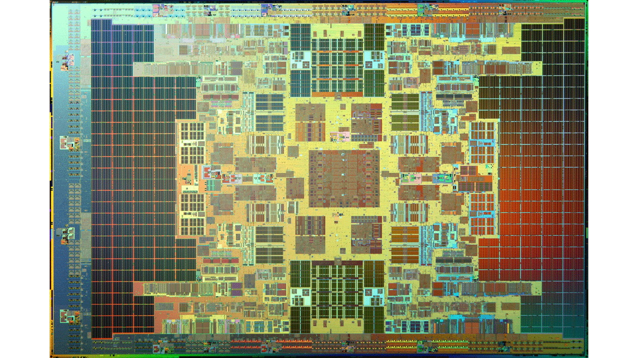
Apologies to its many fine citizens, but there's little to distinguish the berg of Tukwila, Washington, from the maze of similar towns that lie in the urban belt between Seattle and Tacoma. Why then did Intel forever immortalize it as the codename for a generation of Intel Itanium processors? The processor that first cracked the two billion-transistor mark? Only Intel knows for sure. In any case, behold the Tukwila.
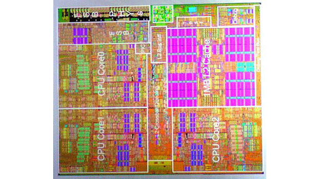
And here we thought gaming machines were different, powered by wee little Marios, forever running on virtual hamster wheels. Perhaps we should have been paying more attention, because gaming publication TeamXbox proved us all quite wrong way back in 2005 when it finagled close-up photos of the processor die of the new holy grail of consoles, the Xbox 360. And here's one of those shots for you, in all its multicolored glory.

Elsewhere in this pictorial we chronicle the adventures of Canadian company Chipworks, whose devoted staff digs deep into various chips to find how they tick. But neither Chipworks or anyone else—including the supposed source, Time Magazine—uncovered this apparent poke at Bill "Sux" Gates, purportedly found in the inner sanctums of a circa 1998 Intel Pentium CPU. It was a hoax pure and simple, but that didn't stop several media outlets from running the story.

 Join The Club


