Intel shares details of a discrete GPU prototype in development
An early look at what a non-integrated graphics solution from Intel might look like.
Keep up to date with the most important stories and the best deals, as picked by the PC Gamer team.
You are now subscribed
Your newsletter sign-up was successful
Want to add more newsletters?
When Intel announced in November that it had hired Raja Korduri, the graphics whiz that spearheaded AMD's Radeon Technologies Group and Vega development, the company made clear that it intended to build "discrete graphics solutions for a broad range of computing segments." No small deal, as we haven't seen a proper discrete graphics solution from the company since the i740 around two decades ago. Now three months later, we're getting a look at what one of Intel's discrete GPU solutions entails.
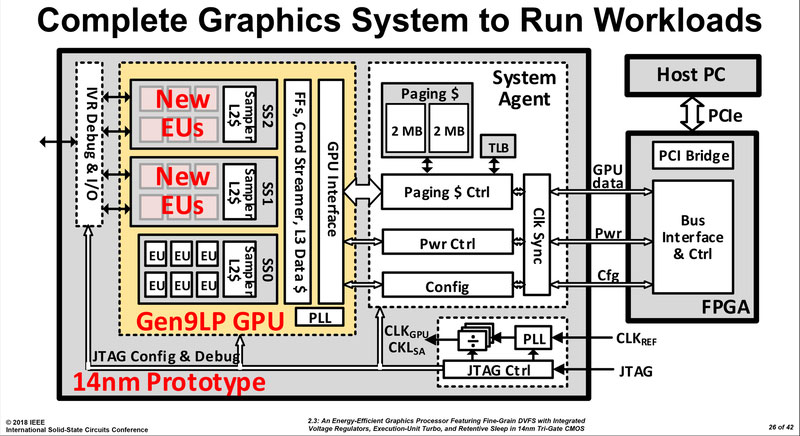
The folks at PCWatch, a tech site in Japan, posted a handful of diagrams shared by Intel at ISSCC (IEEE International Solid-State Circuits Conference) in San Francisco, California. They depict the inner workings of a discrete GPU prototype that Intel is working on. It's not entirely clear how far along Intel is at this point, but it's interesting to take a look at where the company's thinking is at.
Intel's discrete graphics chip is based on Intel's 9th generation graphics architecture, otherwise known as Gen 9 graphics. Don't confuse that with Intel's 9th generation Core CPU architecture codenamed Ice Lake, as they are two entirely different things.
Article continues belowThe discrete GPU is built on a 14-nanometer process and consists of 1.5 billion transistors. To put that into perspective, Nvidia's GP102 GPU that's found in the GeForce GTX 1080 Ti is built on a 16nm process and has 12 billion transistors. The GP108 found in Nvidia's GT 1030 cards meanwhile has a similar 1.8 billion transistors.
All indications are that this is a lower end discrete GPU, likely intended for laptops and maybe systems like the NUC. It's actually a two-chip solution—the first chip contains the GPU and a system agent, and the second chip is an FPGA that connects to the host PC.
As for speeds and feeds, frequencies range from 50MHz at 0.51V to 400MHz at 1.2V. It seems Intel is focusing on power efficiency rather than raw performance, but again, this is a prototype. Final hardware could clock significantly higher.
This is obviously not something that will compete with discrete graphics cards from AMD and Nvidia for gamers. However, there's nothing to say that Intel isn't working on a gaming grade GPU as well. If the design can readily scale (which is pretty common), Intel could be looking at future 12 billion transistor parts. Either way, it will interesting to see how this new part fares against integrated solutions, when and if it comes out.
Keep up to date with the most important stories and the best deals, as picked by the PC Gamer team.
Update
An Intel spokesperson reached out to PCGamer with clarification on what exactly the company shared at ISSCC. Here is the statement in full:
"Last week at ISSCC, Intel Labs presented a research paper exploring new circuit techniques optimized for power management. The team used an existing Intel integrated GPU architecture (Gen 9 GPU) as a proof of concept for these circuit techniques. This is a test vehicle only, not a future product. While we intend to compete in graphics products in the future, this research paper is unrelated. Our goal with this research is to explore possible, future circuit techniques that may improve the power and performance of Intel products."
Paul has been playing PC games and raking his knuckles on computer hardware since the Commodore 64. He does not have any tattoos, but thinks it would be cool to get one that reads LOAD"*",8,1. In his off time, he rides motorcycles and wrestles alligators (only one of those is true).


