Inside Intel: here's what goes into making a cutting-edge gaming CPU
Ever wondered what actually goes on inside a processor fab? I tour Intel's Fab 28 and labs to find out.
One of our favourite pieces from this year, originally published October 31, 2022:
Open-chip surgery is a thing. And it involves ion beams. This came as news to me as I wandered through Intel's lab in Haifa, Israel, and no sooner had I learned about its existence I came face to face with the impressive machine that performs the surgery. It's surprisingly small, quiet even, and it has one of the coolest names imaginable: Focused Ion Beam, or FIB for short.
When it comes to fixing a faulty processor, there's no easy way to do it. I should have known that performing bypass surgery on chips with transistors only nanometers across would require intense effort and precision. Yet it's so easy to disregard what goes into making a chip when you're regularly benchmarking heaps of them like I am.
But as I'm standing in the FIB lab, watching an engineer hone in on a microscopic area inside a chip and alter how it functions with extreme accuracy, the intense effort that goes into each stage of the chipmaking process hits me like a ton of bricks. The fact that any of these chips exist, and we get new ones every single year, is mind boggling.
The reason I'm here at Intel's Israel Development Center (IDC) is to get a glimpse of what it takes to develop, manufacture, and validate a processor. Intel's IDC is where a lot of the legwork takes place in the creation of its processor architectures, including many of those familiar to PC gamers over the years. Skylake, Kaby Lake, Coffee Lake, Ice Lake, Rocket Lake, Alder Lake, and now Raptor Lake chips—these all originate with IDC.
So you could say it's a good place to learn about the intricacies of building a processor from scratch.
IDC
"You have a spare tyre in your car, I have a spare block in my CPU."
Our tour begins at the end: the Post Silicon Validation Lab. This is where engineers team up with manufacturers, OEMs, and partners to ensure that Intel's upcoming chips work well in their systems. While most PC builders will work to their own spec, most large-scale system builders are working to Intel's.
The biggest gaming news, reviews and hardware deals
Keep up to date with the most important stories and the best deals, as picked by the PC Gamer team.
To one side of me, Microsoft Surface laptops with the latest mobile chips. To the other, two Alienware desktops running Raptor Lake. These systems were in the lab in September, so at least a month in advance of the 13th Gen's launch, if not long before our hoard of journalists were bused in.
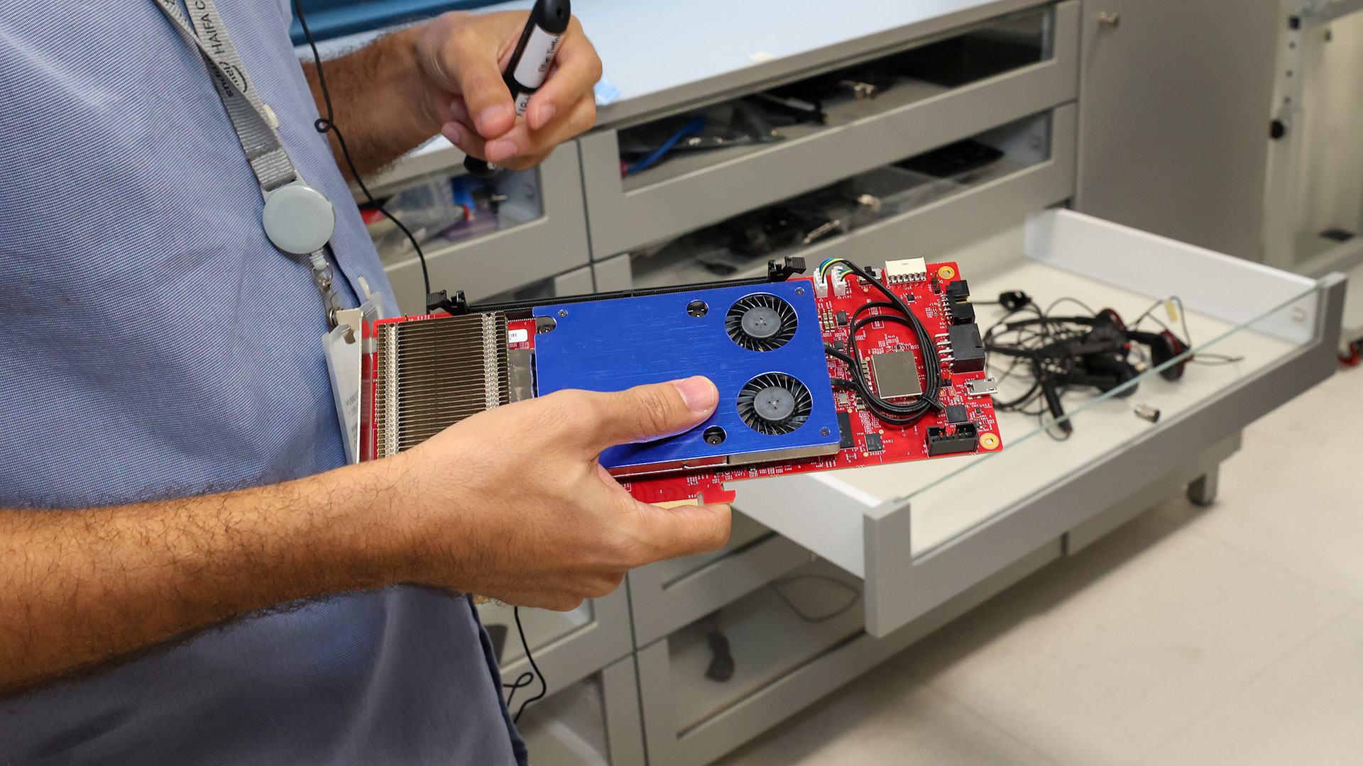
At the end of the room sits a drawer of goodies, including two early Raptor Lake samples. Though what's more out of the ordinary in this lab is the PCIe 5.0 test card. When Intel adopted Gen 5 for its 12th Gen CPUs for the first time, there were no add-in cards capable of utilising Gen 5 ports. Intel had to make one for itself. It seems so obvious in that testing environment that such a device would be required, but I hadn't thought about how testing new features on your unannounced or high-performance products often means building cutting-edge testing vehicles, too. It's not a sleek looking device, but it's not particularly shoddy either, and I'm told it gets the job done.
This validation lab is also where we hear of Alder Lake's first boot on Windows. The 12th Gen chips were the first to use Intel's new hybrid architecture: a slightly less homogenous approach to computing utilising both Performance-cores (P-cores) and Efficient-cores (E-cores) on a single die. This disparate build requires a different approach to OS optimisation, and Intel's engineers made no bones about the hours it took to boot an Alder Lake CPU into Windows for the first time.
The first time Intel booted the chip was from the very building I was standing in. But the 12th Gen chip wasn't. The chip was located over 6,000 miles away in the US. A completely remote first boot.
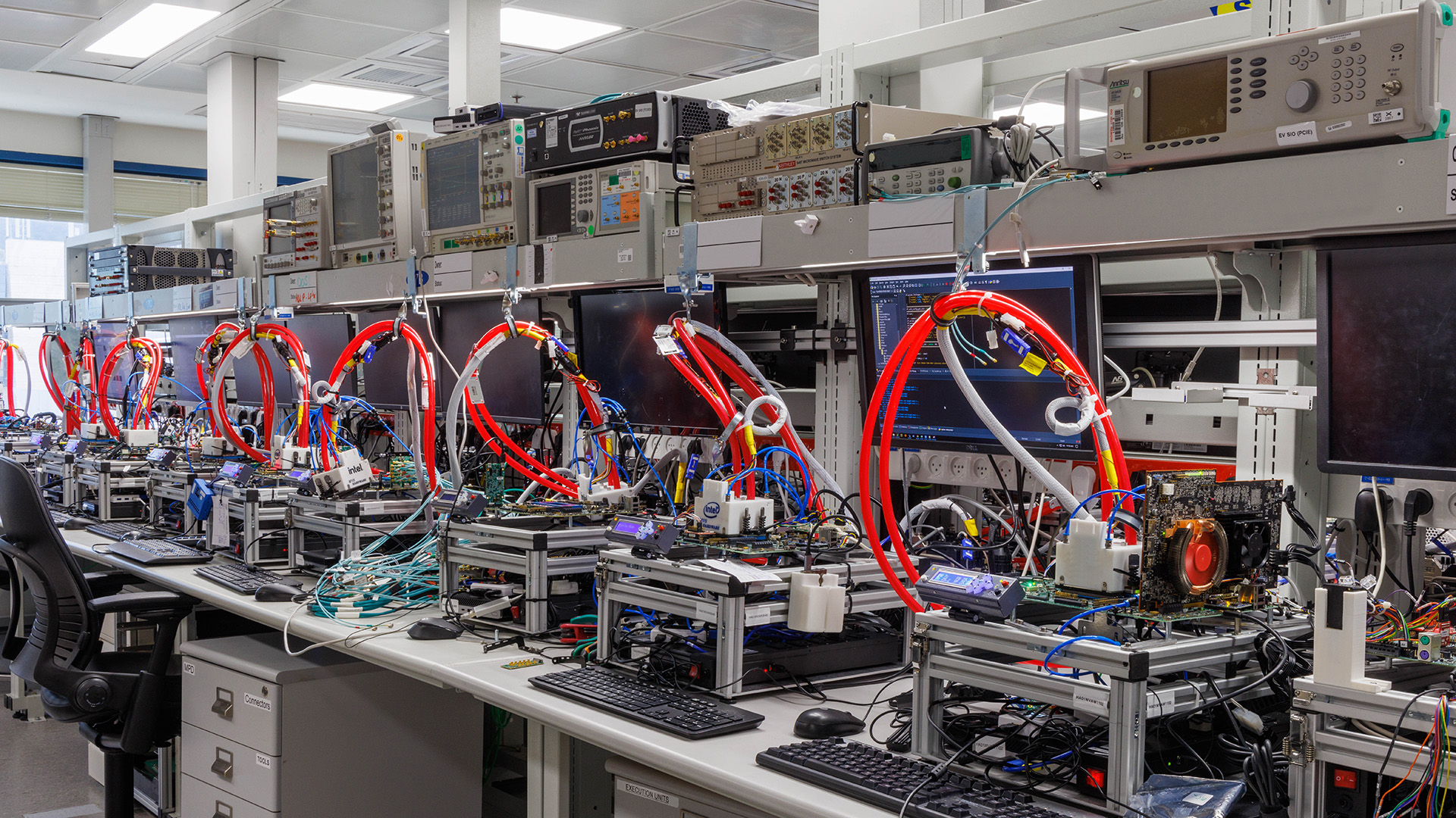
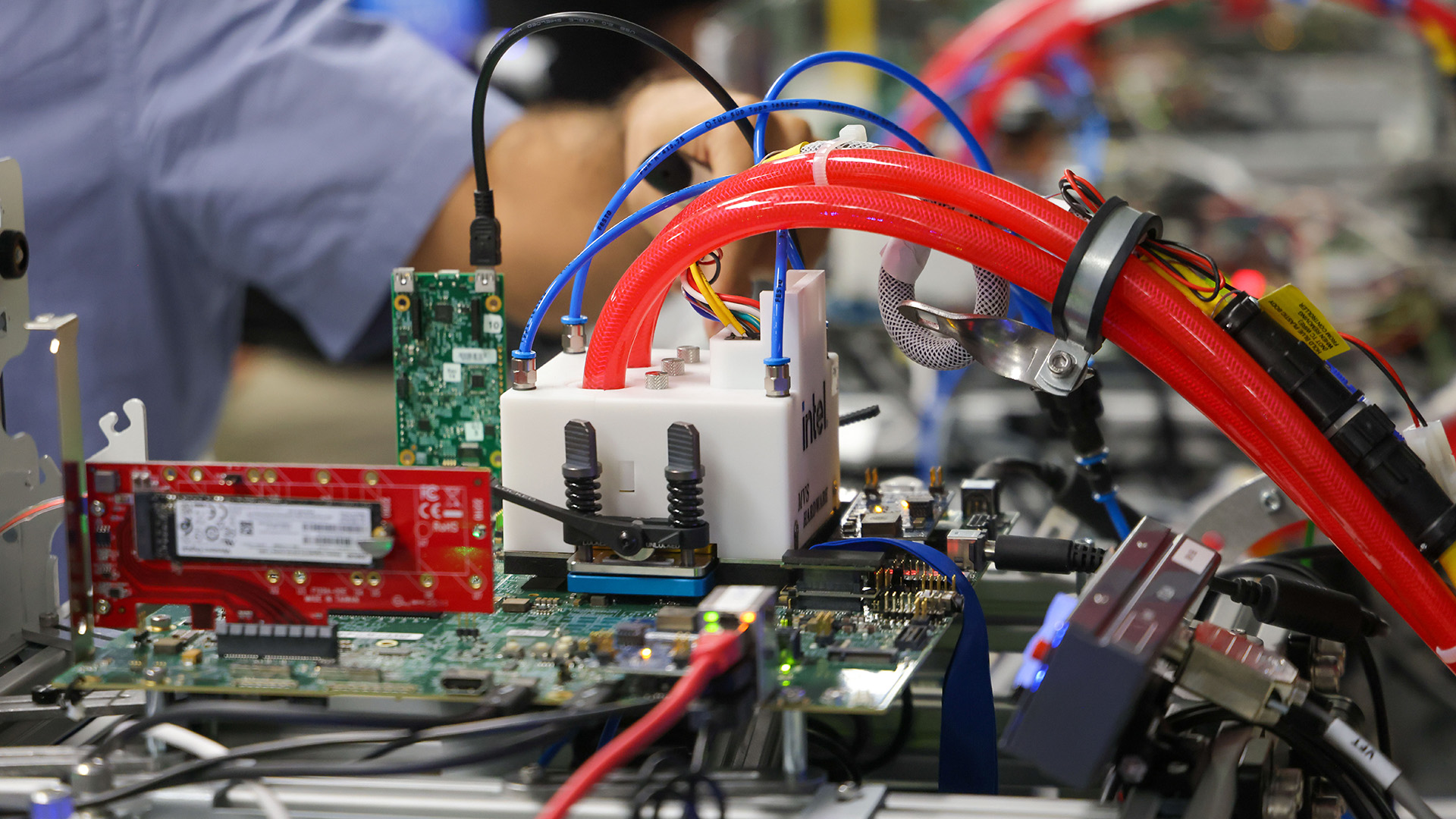
We head out the lab the way we came in, back into a room lined with test benches for aisle after aisle. This is Intel's stress and stability area: where CPUs are put through their paces to see if they're ready to ship or if another stepping is required. Intel has some of the most modular and impressively compact test benches I've ever seen, and I'm only slightly (very) jealous of them. The PC Gamer test benches are a mess by comparison—functional (mostly) but messy. These are gorgeous, modular and compact by comparison.
Intel is running what must be hundreds of systems with bespoke hardware, automated programs, and cooling. The liquid cooling loops throughout Intel's labs are actually plumbed into the wall, for goodness' sake, which is the first time I've seen anything of the sort.
As we're walking through the aisles of test benches, there are heaps of recognisable codenames stuck to each and every one: RPL (Raptor Lake) and ADL (Alder Lake) among them. There is more often than not a familiar benchmark running on a constant pre-programmed loop, too. 3DMark is being used to measure the might of these chips, and we're told that engineering samples from different stages have variable standards set for stability in order to get the go-ahead to move to the next stage of the operation.
Then we're onto power and thermal performance testing, though it's not so much next in a chip's life as it's just where we're ferried to next. I'm told there's plenty of communication between teams and a constant back and forth on samples, so it's less of the one-way street to validate a chip as you might imagine it to be.
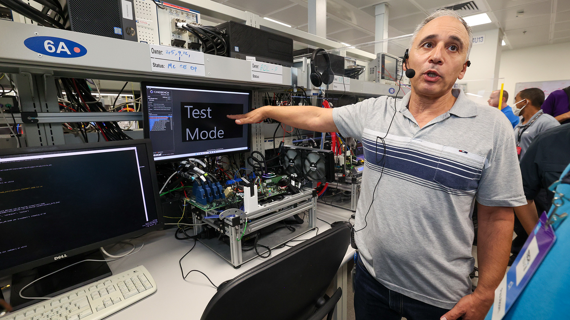
This is where a lot of debugging for future chips happens in regards to applications that customers, like you and me, might actually use.
Gaming is the benchmark of choice for many of the chips being tested while we're in the lab. Here Intel is pairing its CPUs, namely Raptor Lake at this time, with Nvidia and AMD graphics cards. It has a whole lot of them, and lots of consumer motherboards, lining the workbenches alongside accurate thermal and power monitoring tools. A handful of high-end cards were being tested in Shadow of the Tomb Raider while I was in the room, with intermittent monitors flickering to life with graphs showing voltage curves and temperatures.
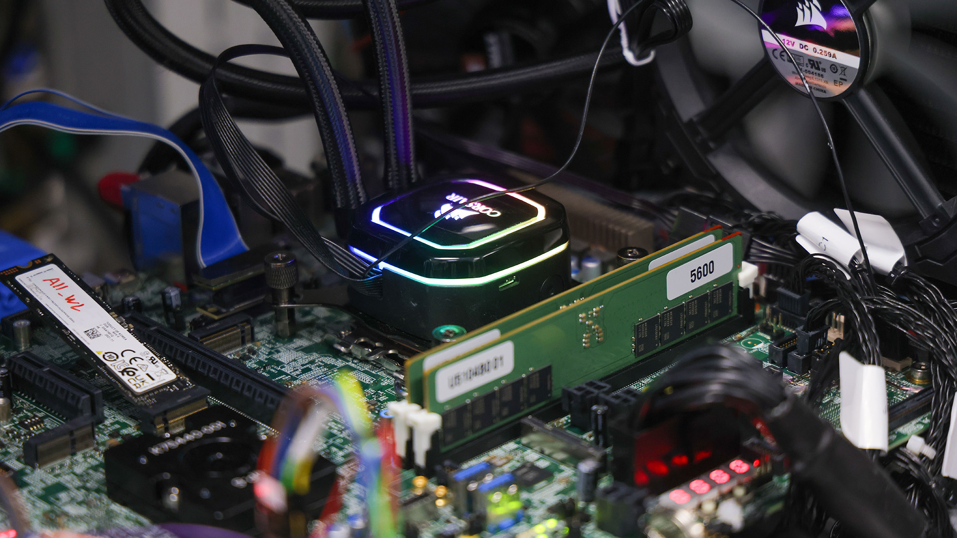
The engineers here are also using standard CPU coolers, to better replicate how these chips will be actually setup out in the wider world.
All roads lead to the Class Test Lab. Every engineering sample spotted in a database or sold on eBay over the past few years once made its way through here. We're told it's the most engineering focused lab at Intel, but it's said with a smirk. It has the desired effect of getting a rise out of our Intel tour guides from other departments, at least.
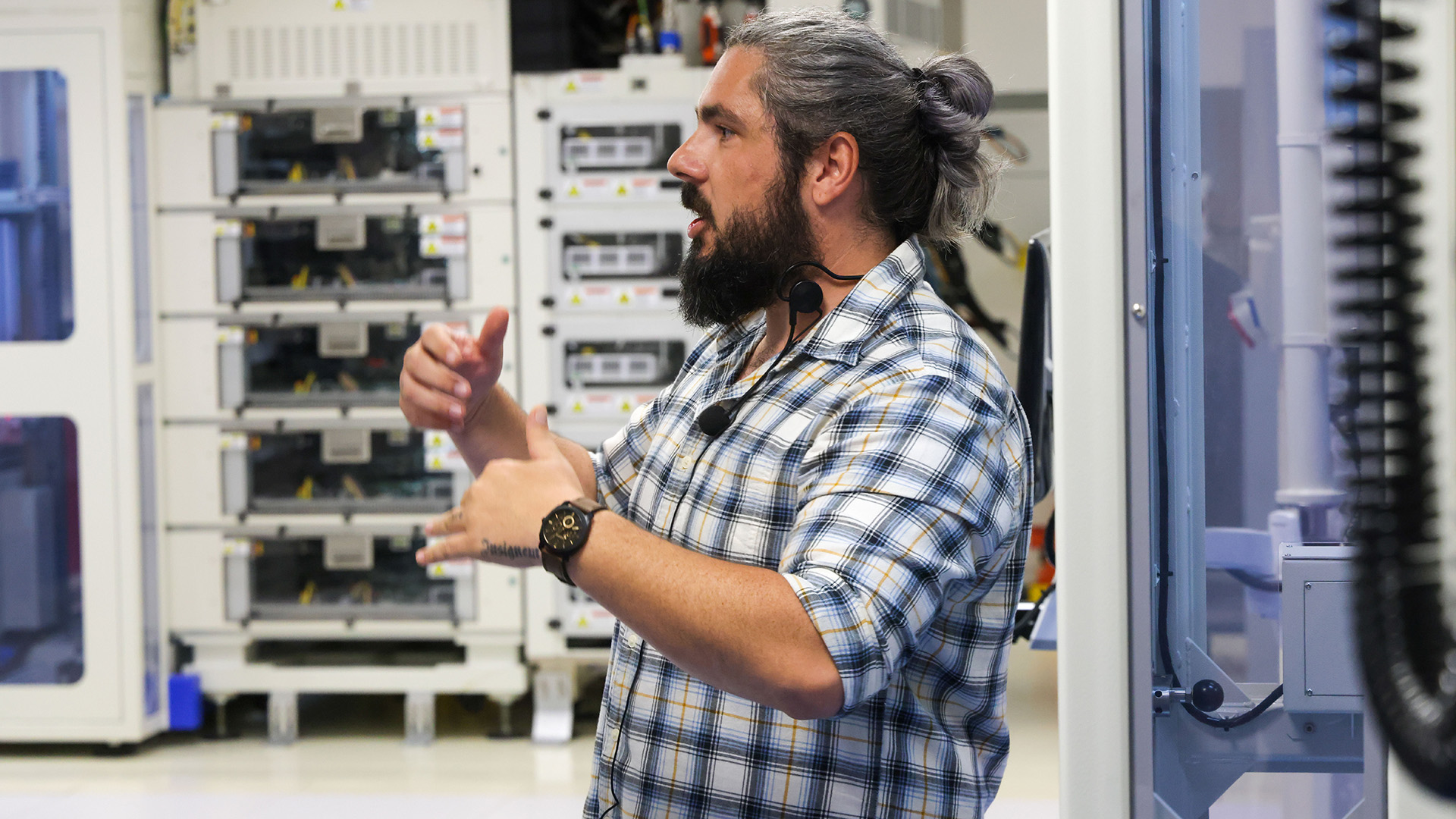
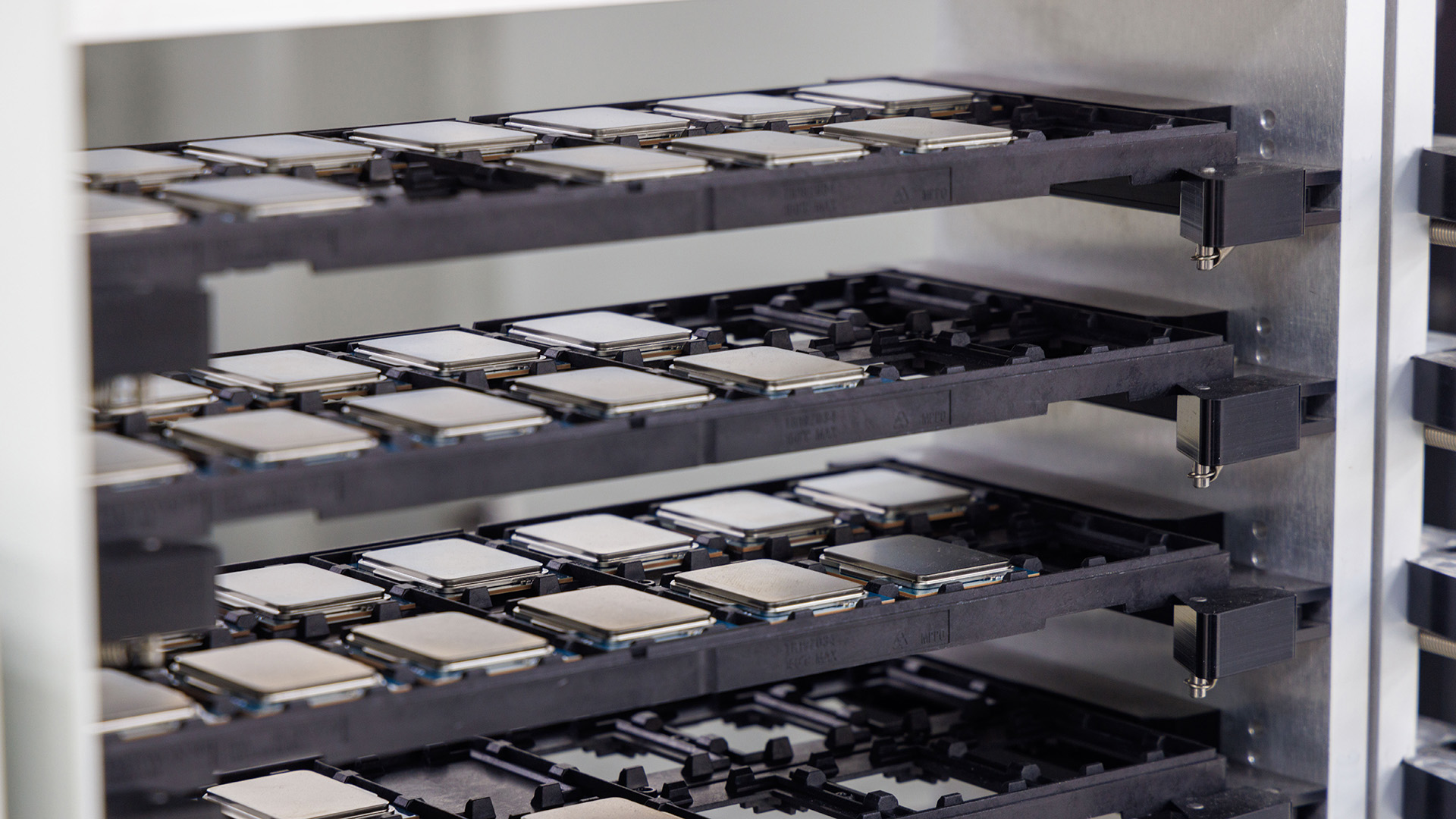
In this lab, which is lined with racks of test machines and containers with multiple generations of samples within, Intel is able to classify blocks independently of each other. "You have a spare tyre in your car, I have a spare block in my CPU," an engineer tells us.
Each block in a CPU is a functional component. They range in size from the smallest of buses to a whole core component. Having the ability to classify these on a block by block level offers flexibility in both construction and troubleshooting, so it's an important step in speeding up the design and validation process.
If it's broken, we'll find it.
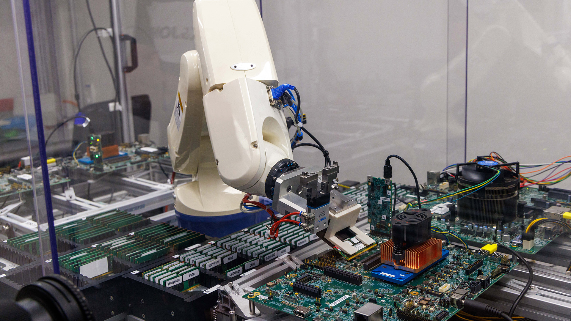
Electrical validation offers another way to check a processor for errors. This is primarily a job for robots, which work through trays of chips, installing them into a motherboard one by one, and run various scenarios and configurations to check for errors. We're stood by some of Intel's older testing tools, which require some human calibration to prevent a robot arm jabbing its suckered finger into the socket. Though close by is a brand new machine. This fancy number, we're told, removes the need for even more human configuration, allowing for swifter, more comprehensive data gathering.
As you might already be noticing, there are many steps to validating a processor before its final design or release. But what happens when one of these steps finds something isn't working as intended? That depends on the error, of course, but when an error is found the chip heads to a department called Component Debug.
"If it's broken, we'll find it," an engineer called Arik tells us.
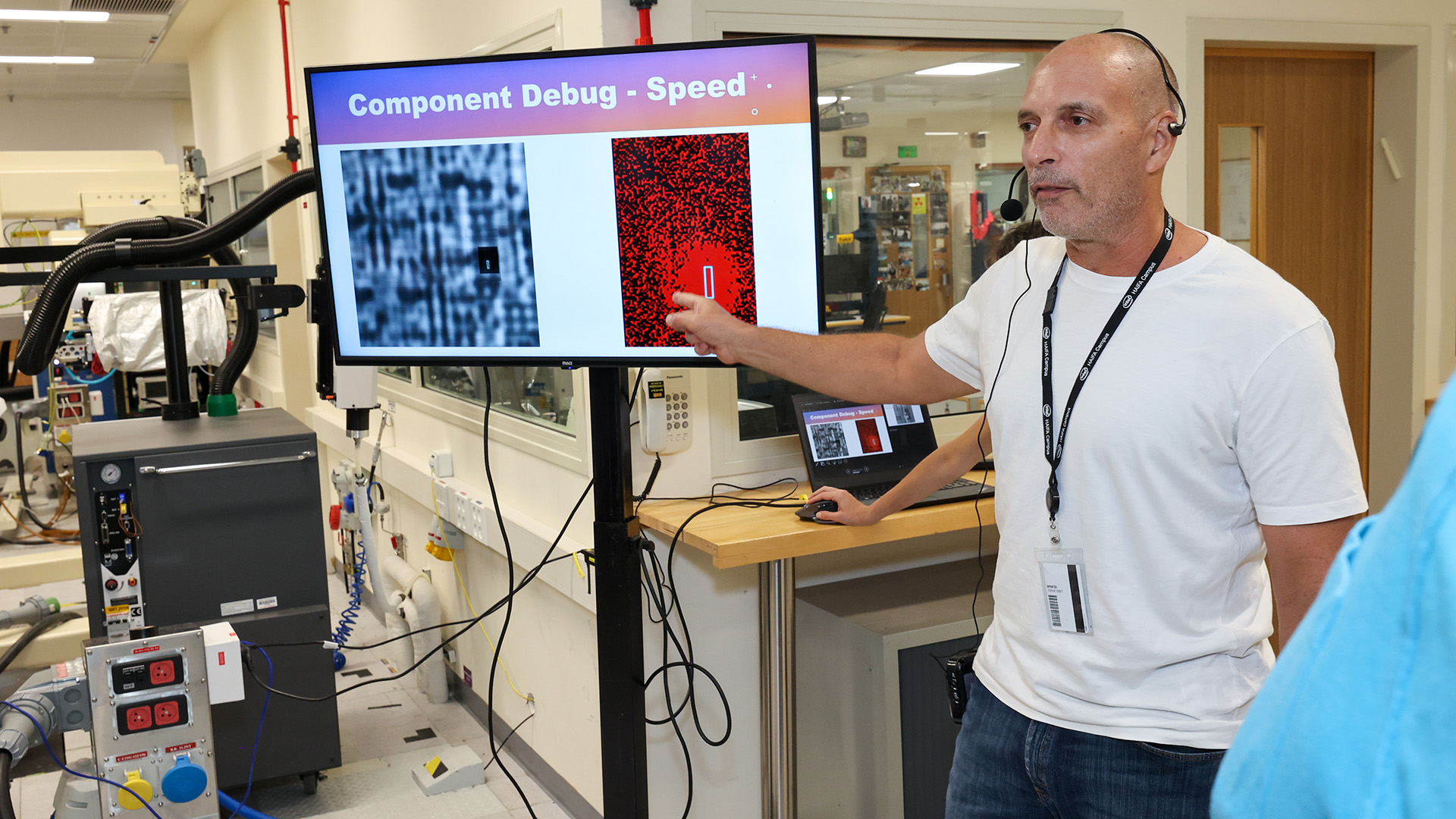
In debug they uncover the root cause of an issue. Say a chip isn't hitting the speed expected of it, to give one example of myriad things that could go wrong with billions of transistors in play, someone has to figure out why. Arik explains to us that in this example they'd be looking for a path that's limiting frequency or causing instability.
To do that, they can scan the CPU with a laser to find areas where something isn't looking right. The image they get back from the scan sort of looks like red noise to me, but I'm no electrical engineer. It's absolutely some sort of electrical divination, but from these splodges of red and black Arik and his team can spot where something doesn't look right. From there they can attempt to devise a permanent fix.
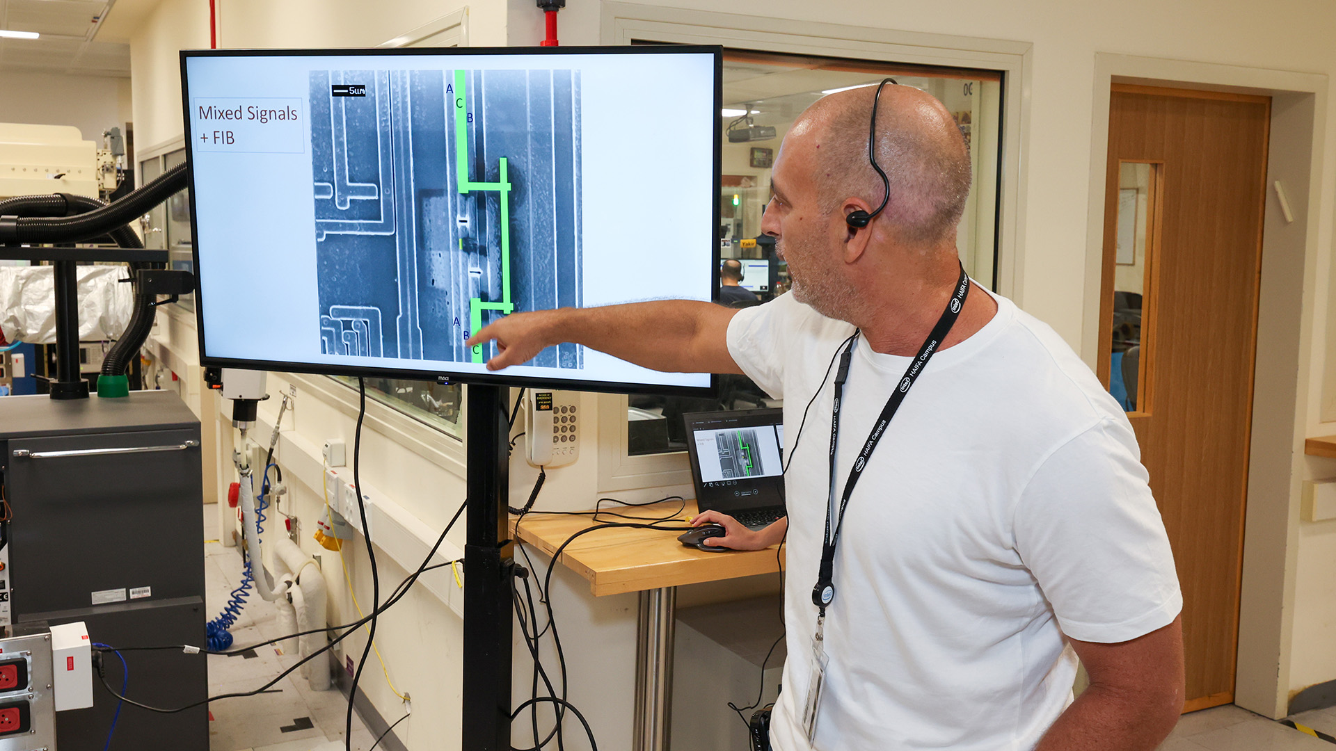
Then it goes to the FIB lab. I began this feature talking about the Focused Ion Beam machine and it's because it blows my mind. The FIB tool sits in the centre of the room. It's smaller than I imagined. This is used to mill a CPU and fire ions on it until it works. Sounds so simple, right?
To fix a CPU, first it has to be milled, creating a tiny upside down pyramid shape in the silicon. This area is tough to see with the naked eye but these systems have an electron microscope at hand to help with that. With a microscopic worksite created, an ion beam is blasted into it to either deposit materials in order to etch a new pathway into the silicon—a tiny bridge, or connection that wasn't there before—or destroy one. It's marvellous.
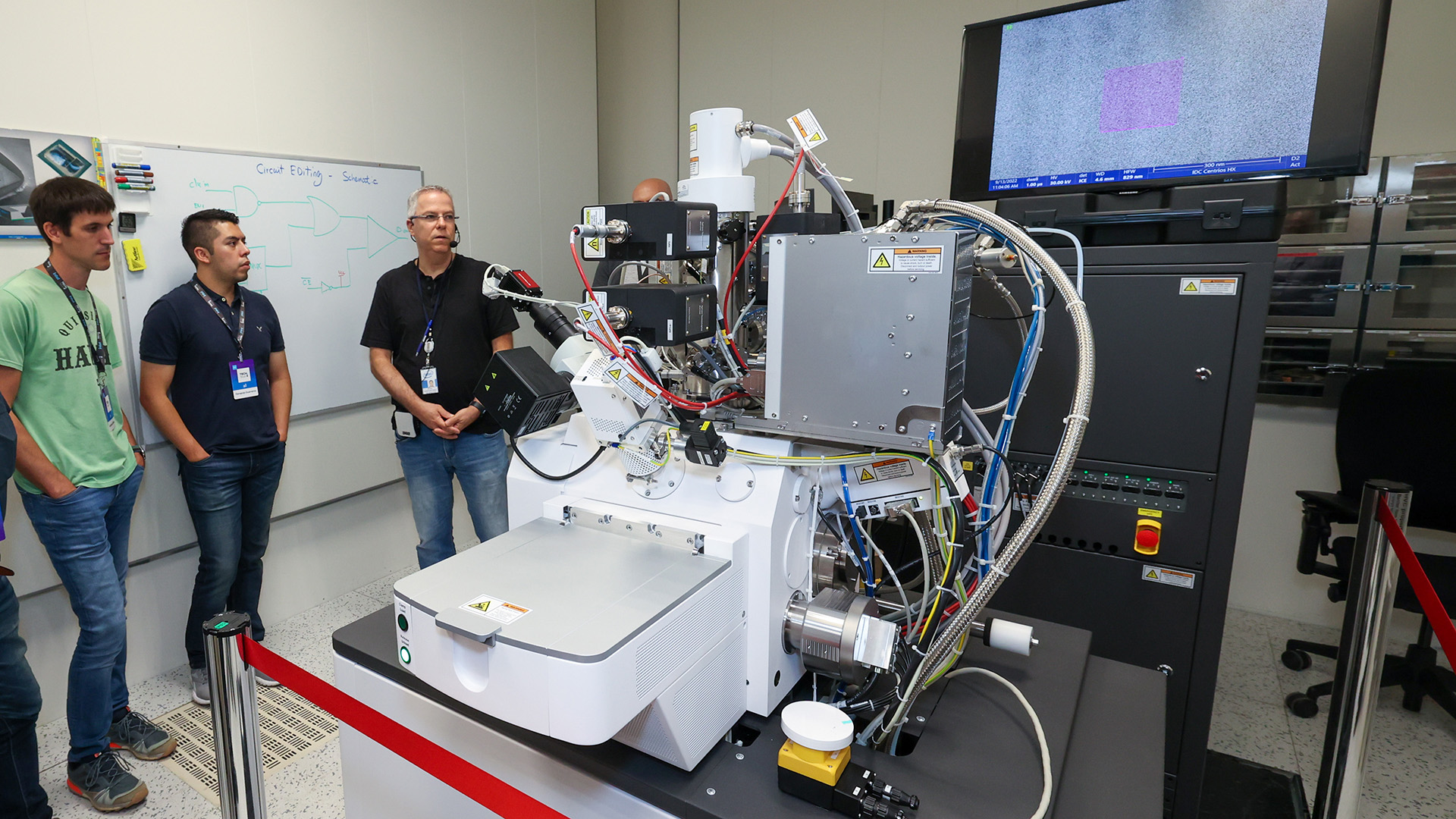
The issues and their potential fixes from debug end up in a bucket of work for a FIB team to look at, patch up, and send back for retesting. The key thing here is that the blueprints for a processor, known as masks, aren't necessarily being changed before a fix is found and tested to ensure it works. This way, when the debug team find a fault and suggest a fix, the FIB lab can etch the fix into a chip at a nanometre level and then fire it back for retesting, If the issue is resolved, great, that's a change for the next stepping of an engineering sample, along with many other fixes.
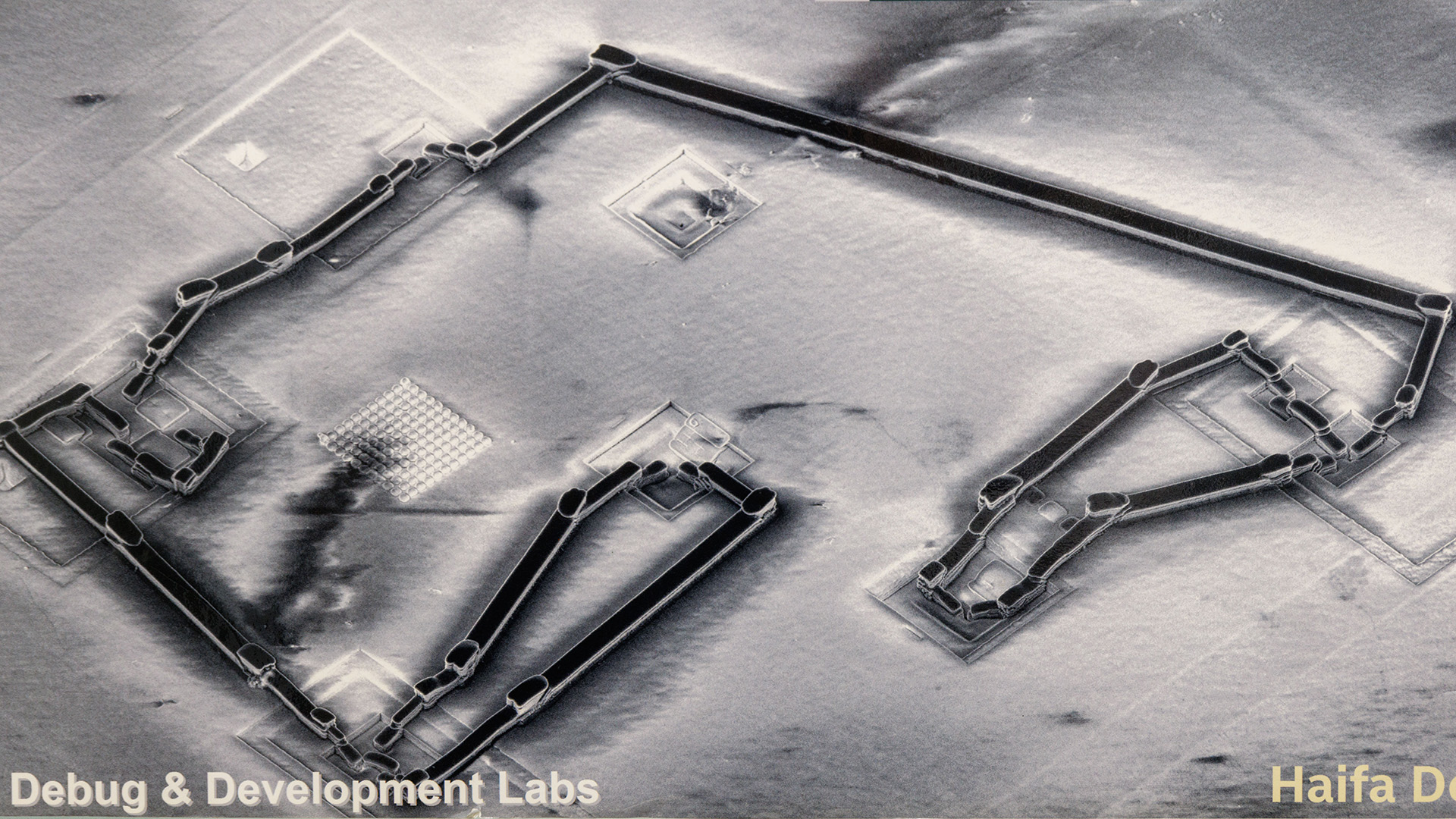
The one thing you have to be extremely careful about in the FIB lab is vibration, however. One small movement could send an ion beam on a destructive path across perfectly fine silicon. Even though the FIB machine is on a vibration-proof section of the floor from where I'm standing, I'm constantly checking my feet don't tread over the edge as I watch someone carry out silicon surgery less than a metre away.
We leave the FIB lab and head back to wrap up the day. At Intel's IDC Haifa lab we've met the people behind validation, design and development for Intel's processors, but to get an idea of manufacturing we need to head down the road, to Fab 28.
Fab 28
"Every die wants to live."
An hour away from Tel Aviv, a few hours from Haifa, just outside a city called Kiryat Gat, is one of Intel's major manufacturing hubs: Fab 28. This is one of few places worldwide with bleeding-edge fabrication capability. It's where I'm given a rare opportunity to not only tour the fab facility, but walk inside the beating heart of a chip fabrication plant, known as the cleanroom.
If you have a 12th Gen or 13th Gen processor in your gaming PC, it may well have come from here. Intel likes to split production of any one chip across multiple locations—eggs in baskets and all that—but a great deal of its top gaming processors come from right here.
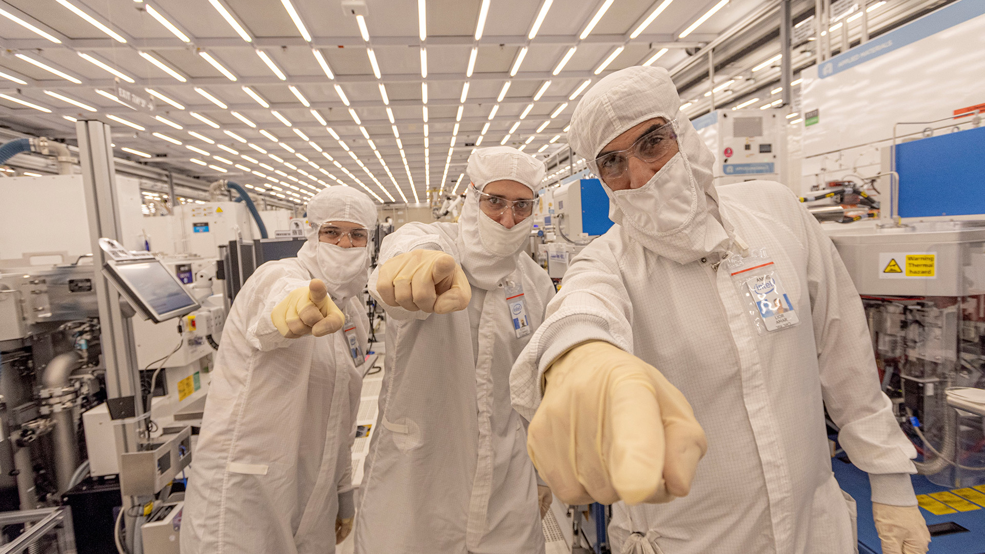
I dare not think of the risk assessment Intel had to carry out to let gaggles of journalists enter its hallowed halls, but, somehow, we were allowed to enter. Above the door, a motto created by the Intel engineering team: "Every die wants to live."
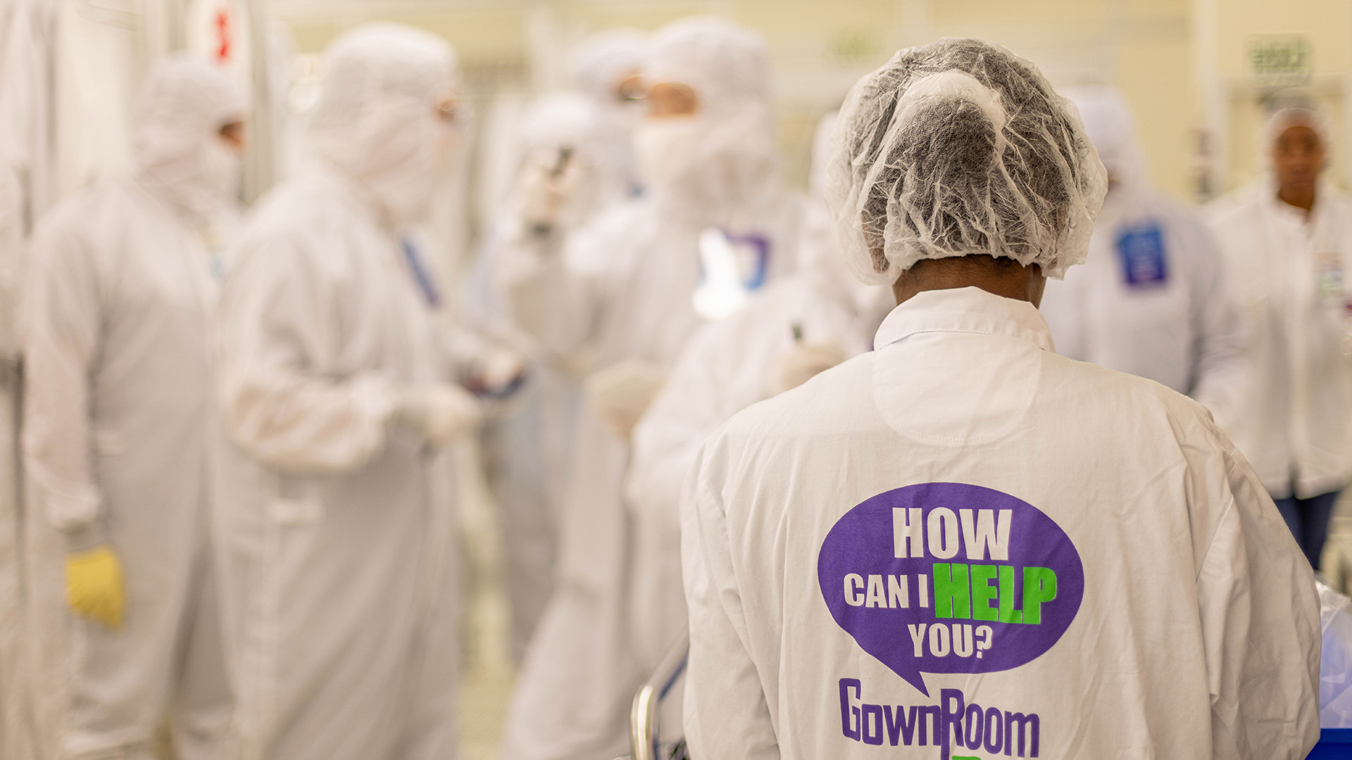
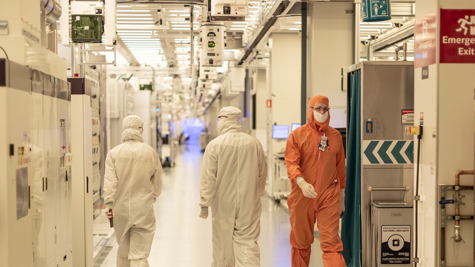
But before I can step foot in the cleanroom itself, I must take the necessary precautions. Intel is serious about no contaminants getting inside the cleanroom, following a few too many issues with dust, crumbs, and pizzas making their way into the fab floor back in the early days. Nowadays Intel has rigorous rules for attire on entry. Hence the bunny suit I'm instructed to don in the gown room before I'm allowed to enter.
The bunny suit has undoubtedly become one of the more famous symbols of Intel throughout its history—just behind the Intel bong. That's bong as in the five-note song played at the end of every Intel advert for years, not the other thing. I don't even know what that is.
Once upon a time these famous protective suits included ventilators that engineers would have to wear for the duration of their 12-hour shifts. Nowadays, the tools each come with their own controlled environment, so they're no longer required. Instead, engineers have to wear only a fabric face mask, hood, hair net, gloves, more gloves, overalls, and tall boots. All of which is washed, stored, reused, or recycled in the gown room in a cordoned off area at the entrance of the cleanroom.
Though the 12-hour shifts remain. In fact, many of those that work in the roles responsible for the day-to-day operations of the fab will work relatively long shifts, including those lining the desks in the control room.
The other thing I'm handed for my cleanroom visit is a specially-made cleanroom safe notepad and pen. You wouldn't think much of them to look at—they're fairly standard looking jotting utensils—but it's a good example of the standards that must be kept to ensure a smooth operation.
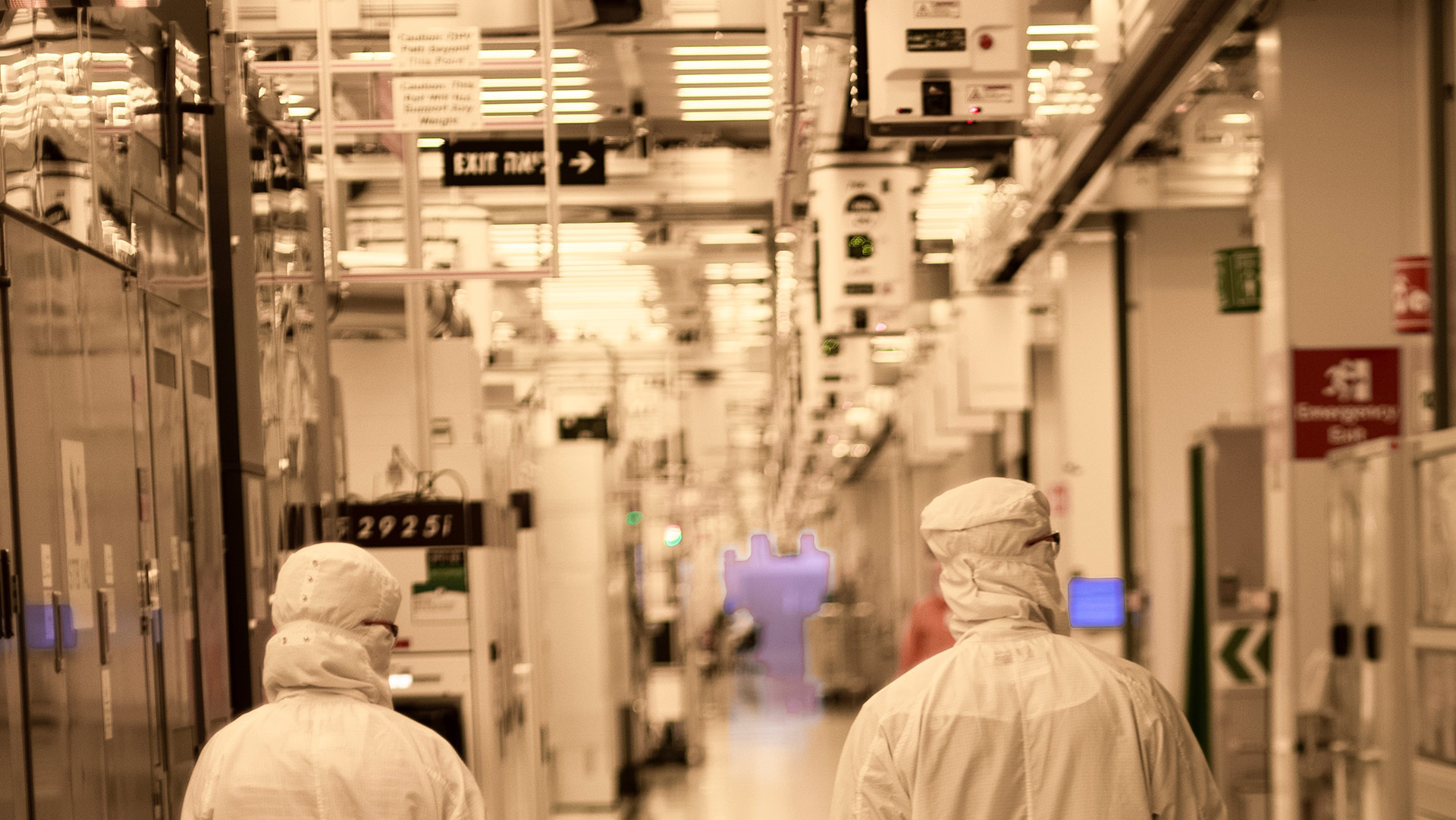
From the preparation area it's a short walk to the cleanroom doors. The first thing I notice as I approach are the lights bathing everything in a yellow glow after them. That's not just for show. Intel uses yellow lights to protect the wafers from harmful rays causing unwanted exposure on the nascent CPUs. This is a factory built to etch wafers with lithography, after all, and that means light is the primary tool with which to go about that.
It's all one big fab.
My first thought upon entering the fab is how gargantuan it is. It goes on seemingly forever in one direction, and we're a football field or two away from the end in the other. Fab 28 is connected up to Fab 18, and to Intel's engineers "it's all one big fab." Someday soon it'll also be connected to Intel's Fab 38, which is currently in construction next door.
Fab 38's floor plan makes Fab 28 look almost small by comparison, but it's largely just steel girders and colossal cranes right now.
My second thought upon entering the fab is slight concern at the wafer bots screeching along above my head. These are known adorably as FOUPs (Front Opening Unified Pods), and you can't see it from the cleanroom floor, but above our heads there's an automated superhighway for FOUPs that can travel at even faster speeds to reach the far ends of the fab. These bots are how all wafers go from point A to point B inside the fab, then onto point C, D, E, F, and so on—there are many stages to the chip making process, and I don't pretend to know them all.
As a stack of wafers is finished in one machine, a FOUP zooms over, two lines descend from under it, the wafers are secured, and it reels them up into its cold, robotic embrace. Then it figures out the best route to take to the next station and zips off thataway. Potentially slowing or stopping on occasion along the way to allow another bot to give way to traffic on a busy intersection.
This system, like most in the fab, is entirely automated, and is a part of Intel's Automated Material Handling System.
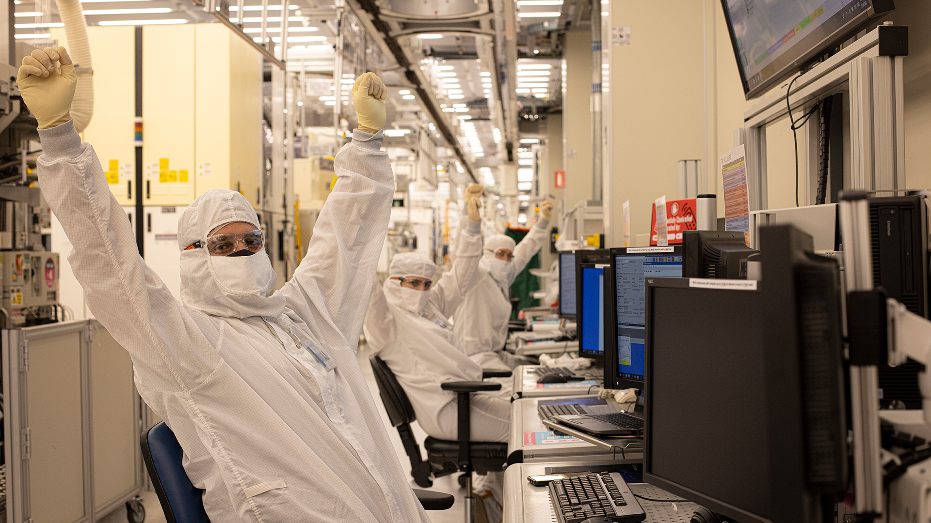
There are also plenty of engineers at work to ensure the fab is functioning properly and efficiently, some of which work in the cleanroom and others that monitor progress from the ROC, or Remote Operation Control—a 24/7 control tower where every two hours the entire staff gets up for some routine stretching to, if my memory serves me, Israeli psychedelic trance duo Infected Mushroom. They say it's really important to them that everyone has a break—they work long 12-hour shifts—but we didn't chance upon this ritual. With a smile, they admit they've been doing it for every group, which works out to roughly six two-hourly stretches in an hour or so.
Next door to ROC—close enough you can hear their psy-trance through the door—is DOR, or Defect Operational Review. This team is the first defence against dodgy wafers, scouring data and harnessing statistics to uncover the cause of defects out of the fab floor. Any issue, however big or small, could come from a number of sources: a specific tool, a process, a material. It's a key job and the relatively small team here take care of all of it.
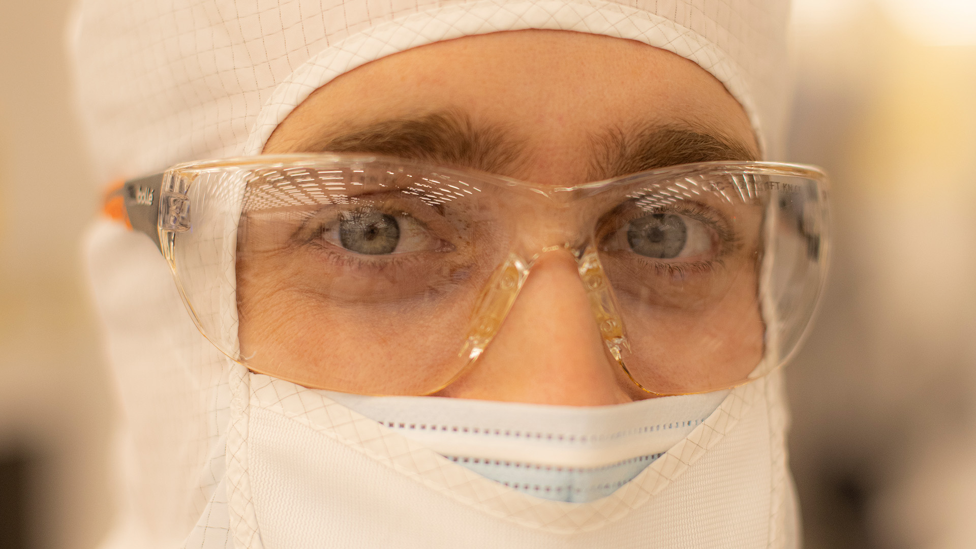
But I'm wrapped up in my overalls for a reason and over in the cleanroom a few friendly engineers took the time out to talk us through the tools and processes they're working on each day. I would think it's a strange place to spend a lot of time, mainly for the yellow lights and bunny suit. But also because you can recognise your coworkers while you're there by only their badge and eye colour.
An Intel engineer explains a few of the key tools surrounding me as we walk further into the fab. It's all frightfully expensive equipment—from the likes of Cymer, Tokyo Electron Limited (TEL), and ASML—but it's the lithographic tools that I'm told are the priciest. At one point we stand next to an ASML Twinscan immersion system, which will cost $100 to $200 million, and we're facing another pricey tool, a TEL Lithius Pro V.
Bear in mind, some of these tools can handle over 200 wafers in an hour, and they're absolutely massive, and there's a seemingly endless amount of them.
If you can believe it, these DUV tools are on their way out, and the next-generation will require even more space and cost that much more money. Hence why Fab 38 is springing up next door. The next few nodes from Intel will require masses of EUV machines, for Extreme Ultraviolet, and will allow for the progress to smaller and more efficient process nodes.
Location: Kiryat Gat, Israel
Opened: 2008
Wafer size: 300mm
Primary node: Intel 7
Gaming processors made here: 12th and 13th Gen Core processors
Yet one tool used inside the cleanroom might be more familiar to us PC gamers, and that's the Microsoft HoloLens set up nearby. Unlike your VR headset gathering dust in the corner, the Intel team actually uses this kit for training new staff. A routine job is pre-programmed in by a more experienced member of the team and the new staff member has prompts, images, and explanations so they may better learn the process on the job.
AR training is a relatively new addition to the cleanroom. Intel introduced it just a few months before the outbreak of the Covid-19 pandemic in 2020, which by most people's opinion is pretty good timing.
And with that our time in the fab comes to a close. A short trip through a very long building, but you could spend all day in there just rooting around the maze of tools.
Yet the cleanroom is just one slice of the fab. There's also the roof space, where the cleanroom's controlled environment is maintained; the sub-fab, which houses the important facilities for power management, chemicals, etc.; and then the dirty utilities floor below that, which as you might imagine houses all the less sanitary power and waste facilities. Four floors total.
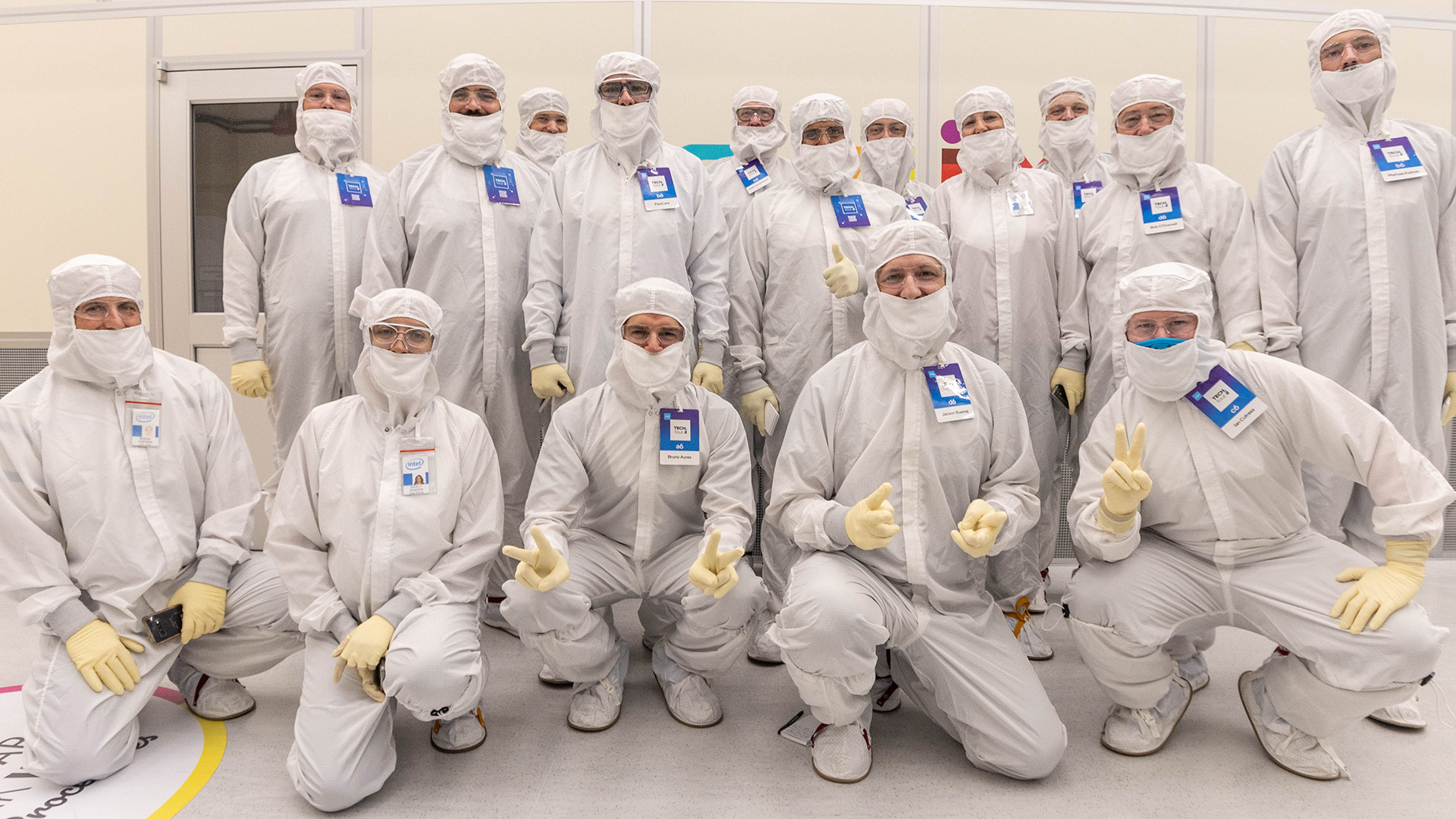
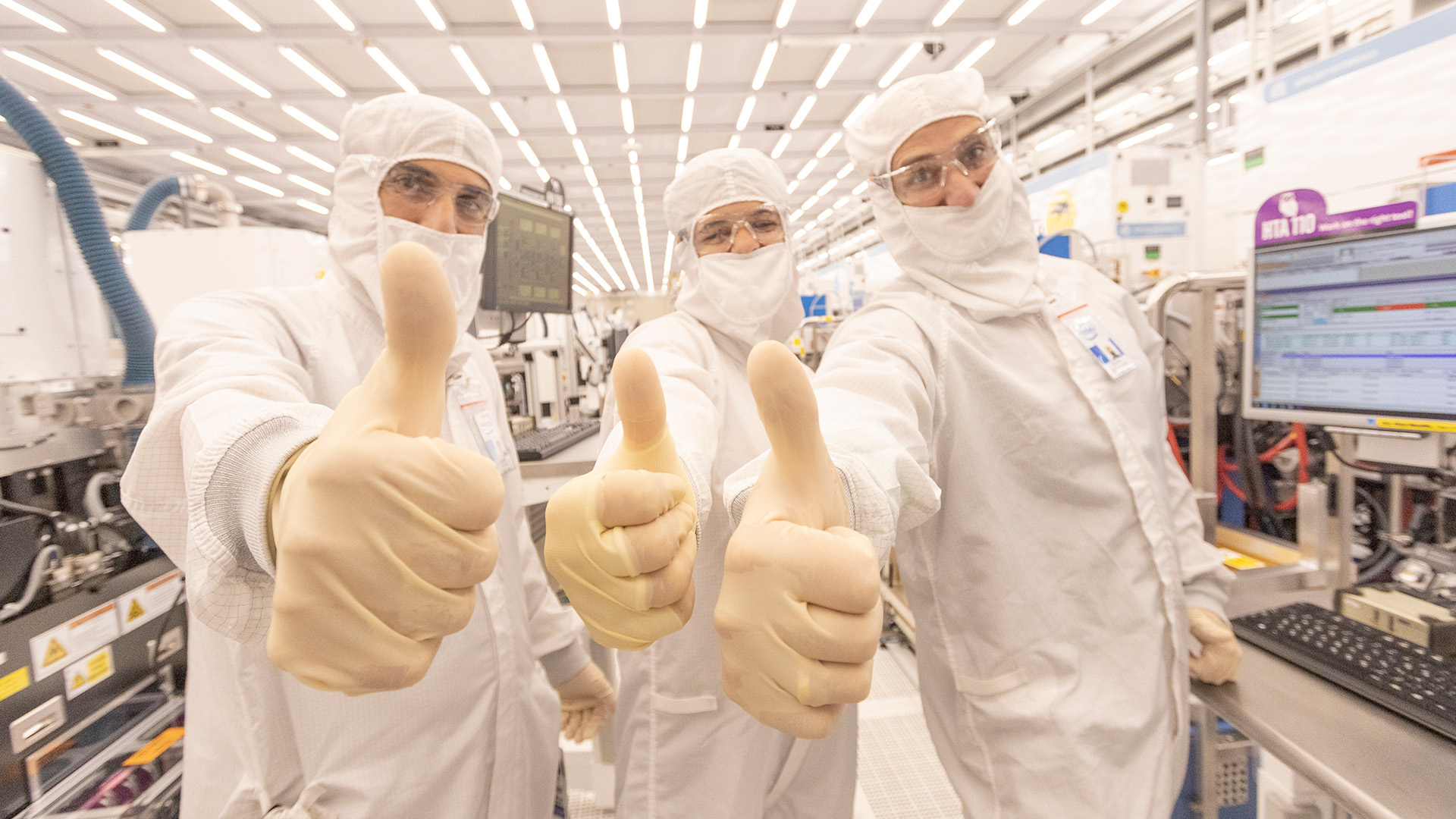
As we walk out from the yellow light and back to the gown room to get back into our civvies, we take a snap. I'm at the back, on the right of the photograph, feeling pretty content. Life goal achieved.
Fab 38

Fab 38—10 bigger than Fab 28
Fab 28 is big. Fab 38 is massive. When Fab 38 is completed, it will house tools capable of delivering EUV-based process nodes, which won't come a moment too soon for the next generation of processors.
EUV technology offers to dramatically reduce the complexity of making a modern processor and continue the descent into smaller and more efficient nodes. Up until now, engineers have been working tirelessly to find new ways to stuff more transistors into a given area of silicon with existing 193nm technologies. That means tricking a 193nm lithographic source into producing a much denser and efficient product. They've generally been quite successful at it, too, using multi-patterning and masks to get the desired results. But it involves more steps, more ways for things to go wrong, and generally will continue to get more expensive as time goes on.
That wouldn't be very 'Moore's Law is alive and well', would it? So Intel, and its like-minded competition, has other plans: EUV.
EUV uses extreme ultraviolet wavelengths that are roughly equivalent to a 13.5nm source, cutting out a heap of extra steps and improving yields. Basically, saving a whole lot of time and money. It was, once upon a time, considered too difficult to ever really work in practice. However, that's a challenge most boffins couldn't resist, and lo and behold we're now on the precipice of EUV process nodes from all the major chipmakers, including Intel, TSMC, and Samsung. The impossible is becoming reality.
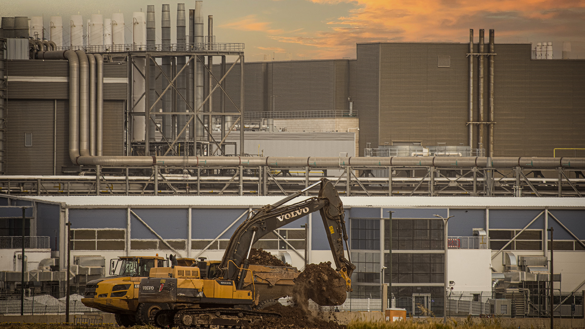
The shift to EUV is still a massive undertaking, however. Not the least bit because these machines are somehow even more pricey than the ones they replace. The other challenge is where do you put these machines: they're bigger than ever, partially due to requiring even more controlled environments to function, and they won't easily fit where older machines exist today.
The answer: you have to build a big new fab to house them. And that's exactly what Intel's doing with Fab 38, and its other new fab developments in Germany and the US.
But Fab 38 is nowhere near ready to build chips yet. What I'm staring at from across the top of a multi-story car park is primarily the foundations of a very expensive building, wrought from thick girders of metal and up to 42 metres into the Earth.
Every square metre matters in a fab. Intel avoids having pillars in the fab for this reason, and instead uses a metal frame circumventing the outer walls of the building. It's not a cheap design decision, nor is it an easy one to carry out. In fact, Intel has hired the world's second largest crane to lift the constituent parts of this metal frame into place.
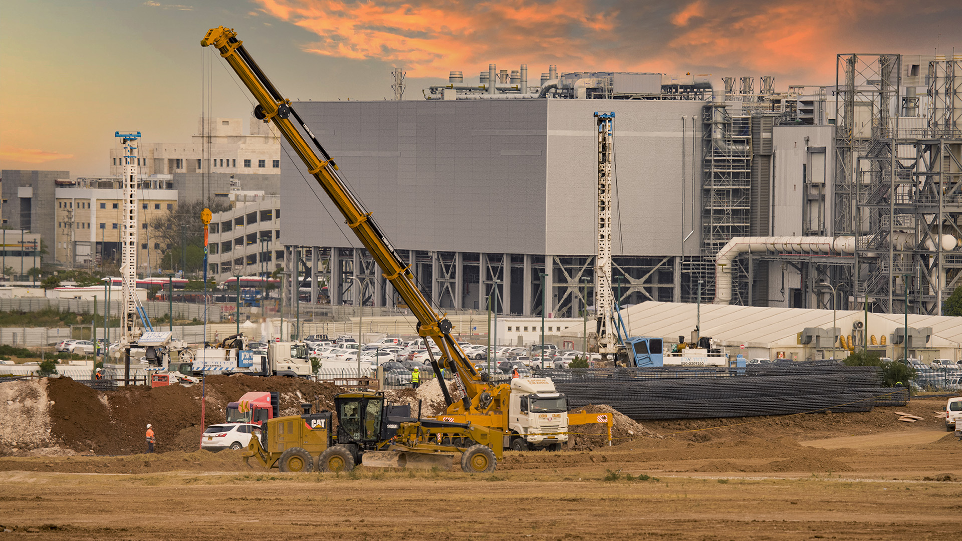
I'm told Intel had wanted the world's biggest crane, but that it was busy building a nuclear power plant in the UK. So it had to settle for the second-largest. Our guide tells us that even this crane costs hundreds of thousands of dollars to operate each day.

Best CPU for gaming: The top chips from Intel and AMD
Best gaming motherboard: The right boards
Best graphics card: Your perfect pixel-pusher awaits
Best SSD for gaming: Get into the game ahead of the rest
The other key ingredient for the fab is concrete. The construction requires so much that Intel has three concrete factories set up dedicated to getting it to the site. To get the concrete from these sites to the fab construction, a large fleet of trucks is required. That causes another issue: congestion. Israel's main highways and roads seem in good enough condition, and on our travels it looks like they're building a lot more of them, but we did get stuck in traffic a handful of times. To try and avoid causing that logistical nightmare, and to not make matters worse for those nearby, Intel's concrete trucks only travel at night.
The exact date when the fab will be finished isn't set, but it'll be ready sometime in the middle of the decade. Likely it'll miss out on the first wave of EUV processes out of Intel, with Intel 4. It takes so long to build new capacity, Intel is essentially betting on demand many years in advance of when it'll come. It's a forecasting nightmare: we're just off the back of unprecedented demand for silicon and now we're in a period of a relatively slow market for processors.
But if another such wave of demand for chips comes again in the future, Intel says it will be prepared. Fab 38 has more room to grow if needed, it's just a matter of when it can hire an extremely large crane.

Jacob earned his first byline writing for his own tech blog. From there, he graduated to professionally breaking things as hardware writer at PCGamesN, and would go on to run the team as hardware editor. He joined PC Gamer's top staff as senior hardware editor before becoming managing editor of the hardware team, and you'll now find him reporting on the latest developments in the technology and gaming industries and testing the newest PC components.

