Here is how Nvidia can sidestep Moore’s Law in GPU design
Packing more transistors into a monolithic GPU won't be feasible for much longer.

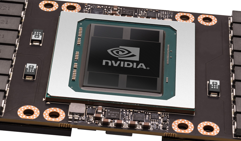
Nvidia is fast approaching a technical wall in GPU design where it will no longer be able to shove more transistors into a GPU die to increase performance at the same rate customers have grown accustomed to. Simply put, as Moore's Law slows down, the number of transistors per die no longer grows at historical rates, Nvidia notes. The solution to this problem could lie in switching to a multi-chip module GPU design.
Researchers from Nvidia, Arizona State University, the University of Texas, and the Barcelona Supercomputing Center have published a paper outlining the benefits of multi-chip module GPUs. It is a design that is working for AMD with its Ryzen CPUs, and likewise Nvidia believes it could benefit GPUs as well.
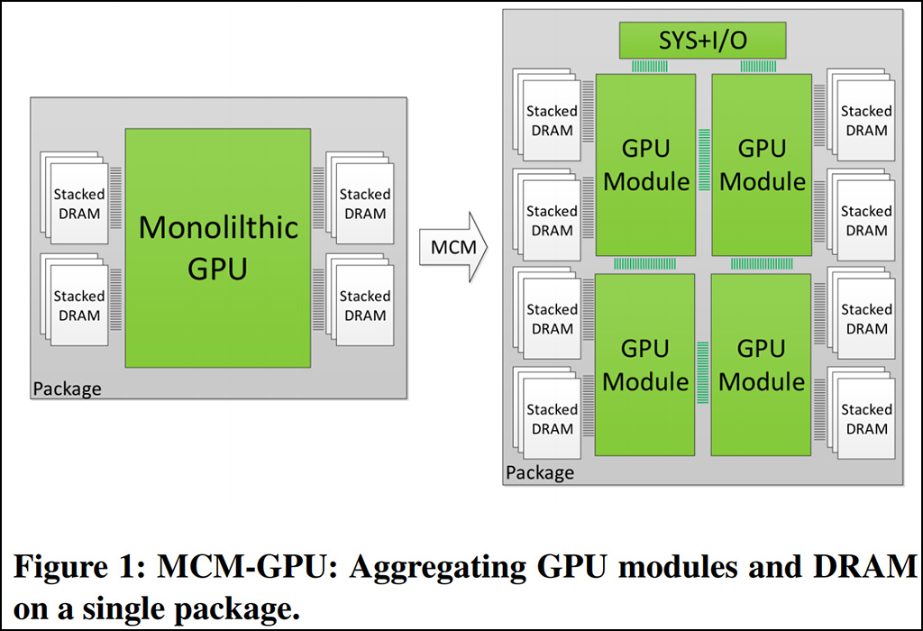
"Specifically, we propose partitioning GPUs into easily manufacturable basic GPU Modules (GPMs), and integrating them on package using high bandwidth and power efficient signaling technologies," Nvidia says.

Without either switching to a multi-chip module design or coming up with an alternative solution, Nvidia warns that the performance curve of single monolithic GPUs as currently constructed will ultimately plateau. Beyond the technical challenge of cramming more transistors into smaller spaces, there is also the cost to consider, both in terms of technical research and reduced die yields.
Whether or not an MCM design is ultimately the answer, Nvidia thinks it is at least worth exploring. One thing that Nvidia mentions in its paper is that it's difficult to scale GPU workloads on multi-GPU systems, even if they scale well on a single GPU.
"This is due to to multiple unsolved challenges related to work partitioning, load balancing, and data sharing across the slow on-board interconnection network. However, due to recent advances in packaging and signaling technologies, package-level integration provides a promising integration tier that lies between the existing on-chip and on-board integration technologies," Nvidia says.
What Nvidia proposes is connecting multiple GPU modules using advanced, high-speed input/output protocols to efficiently communicate with each other. This would allow for less complex (and presumably cheaper) GPU modules compared to a monolithic design. It is a sort of strength in numbers approach.
Keep up to date with the most important stories and the best deals, as picked by the PC Gamer team.
Nvidia's team of researchers used an in-house simulator to evaluate their designs. What they did was build two virtual GPUs, each with 256 streaming multiprocessors (SMs). One was based on the current monolithic design and the other used an MCM design.

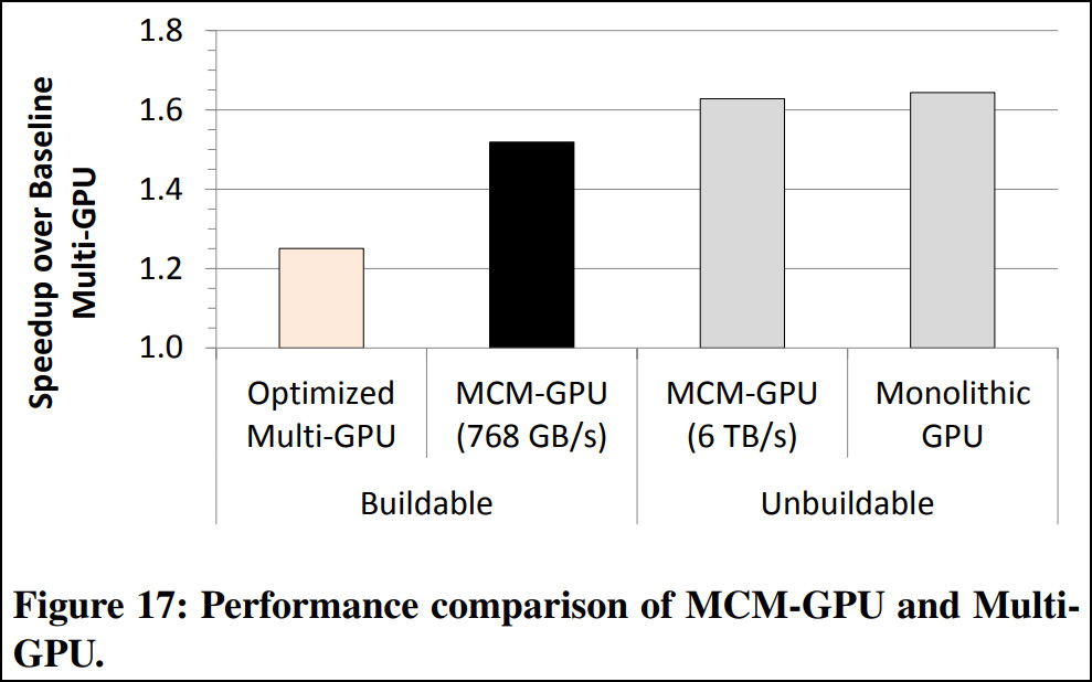
The simulator showed the MCM design performed within 10 percent of monolithic GPU. It also showed that the MCM design would be nearly 27 percent faster than an SLI setup with similar specs. And when optimized, the MCM design can achieve a 45.5 percent speedup compared to the largest implementable monolithic GPU, which would have 128 SMs.
Much of this is hypothetical, not just in the simulation but also the examples used. A 256 SM chip just isn't possible at the moment—Nvidia labels it as "unbuildable." To put that into perspective, Nvidia's GeForce GTX 1080 Ti sports 28 SMs.
It remains to be seen what Nvidia will do for the next couple of generations, though a move to MCM GPUs seems almost inevitable. The question is, which company will get there first? It is believed that AMD's Navi GPU architecture off in the distance could utilize an MCM GPU design as well, especially now that AMD has the tech in place with Zen (Ryzen, Threadripper, Naples, Epyc).
For now, you can dive into Nvidia's white paper (PDF) for all of the gritty details.
Paul has been playing PC games and raking his knuckles on computer hardware since the Commodore 64. He does not have any tattoos, but thinks it would be cool to get one that reads LOAD"*",8,1. In his off time, he rides motorcycles and wrestles alligators (only one of those is true).


