From Voodoo to GeForce: The Awesome History of 3D Graphics
Nvidia GeForce 7 Series
AGP made its last stand in the Nvidia camp with the GeForce 7 Series; every chipset that came after would only come in PCI-E form. And as had become the norm by this time, 7-series videocard would come in a wide variety of speeds and specifications, including integrated graphics.
At the higher end, the 7800 GTX would comprise 302 transistors and a 333 mm 2 die size. This was the first 7-series GPU Nvidia released and it would remain the flagship part until the 7900 GTX showed up almost a year later. The 7900 GTX carried a massive (for the time) 512MB frame buffer, 24 pixel shader units, 16 ROPs, and a whopping 54.4GB/s of memory bandwidth.
The 7-series also introduced dual-GPU videocards in the 7900 GX2 and 7950 GX2. While these would fit in a single PCI-E slot, they were both essentially two videocards sandwiched together. This proved a popular option for gamers who wanted a two-videocard solution but lacked an SLI-compatible motherboard.
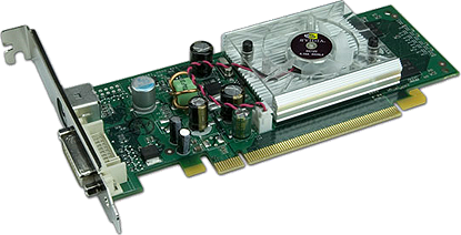
(Image Credit: hwspirit.com)
Model: GeForce 7300 GS
Date Released: 2006
Interface: AGP/PCI-E
Shader Model: 3.0
DirectX: 9
Manufacturing Process: 90nm
Core Clockspeed: 550MHz
Memory Clockspeed: 810MHz
Memory Bus: 128, 256, and 512bit
Transistors: 90 million
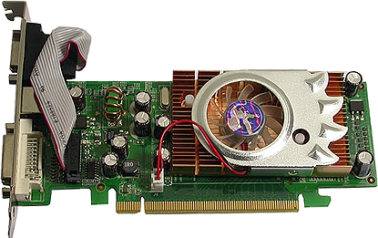
(Image Credit: hwupgrade.it)
Model: GeForce 7500 LE
Date Released: 2006
Interface: PCI-E
Shader Model: 3.0
DirectX: 9
Manufacturing Process: 90nm
Core Clockspeed: 550MHz
Memory Clockspeed: 800MHz
Memory Bus: 256 and 512-bit
Transistors: 112 million
The biggest gaming news, reviews and hardware deals
Keep up to date with the most important stories and the best deals, as picked by the PC Gamer team.
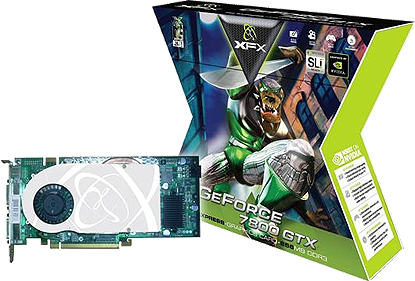
(Image Credit: fsplanet.com)
Model: GeForce 7800 GTX
Date Released: 2005
Interface: PCI-E
Shader Model: 3.0
DirectX: 9
Manufacturing Process: 90nm
Core Clockspeed: 430MHz
Memory Clockspeed: 1200MHz
Memory Bus: 256 and 512-bit
Transistors: 302 million
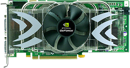
(Image Credit: techpowerup.com)
Model: GeForce 7900 GTO
Date Released: 2006
Interface: PCI-E
Shader Model: 3.0
DirectX: 9
Manufacturing Process: 90nm
Core Clockspeed: 550MHz
Memory Clockspeed: 800MHz
Memory Bus: 512-bit
Transistors: 278 million
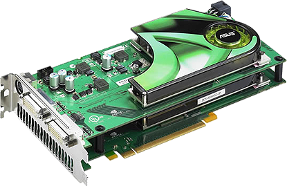
(Image Credit: tech2.in.com)
Model: GeForce 7950 GX2
Date Released: 2006
Interface: PCI-E
Shader Model: 3.0
DirectX: 9
Manufacturing Process: 90nm
Core Clockspeed: 500MHz
Memory Clockspeed: 1200MHz
Memory Bus: 512-bit
Transistors: 278 million
ATI Radeon R600
For the R600, ATI drew inspiration from the Xenos GPU it had developed for the Xbox 360 console. Like the Xbox 360, the PC version consisted of a unified shader architecture rather than relying on separate processors for each task. This modern design also boasted DirectX 10, Shader Model 4.0, and full OpenGL 3.0 support.
ATI retained the Ultra-Threaded Dispatch Processor technology it used in the R520, as well as the same general memory controller design. However, bandwidth was almost doubled as a result of a bi-directional 512-bit memory bus on the HD 2900 Pro and XT. This led to very good performance overall, but it couldn't topple the best Nvidia had to offer.
This was again the case when ATI released the R670-based HD 3870. Performance was excellent for the price, but ATI had all but conceded the high end market to Nvidia. It came as little consolation that the new part added support for DirectX 10.1.
Fun Fact: ATI's dual-GPU HD 3870 X2 became the first single-videocard to reach the 1 TFLOP milestone.
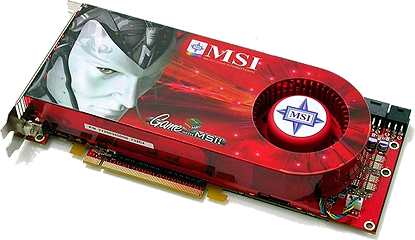
(Image Credit: vr-zone.com)
Model: Radeon HD 2900 XT
Date Released: 2007
Interface: PCI-E
Shader Model: 4.1
DirectX: 10
Manufacturing Process: 80nm
Core Clockspeed: 743MHz
Memory Clockspeed: 1000MHz
Memory Bus: 512-bit
Transistors: 720 million
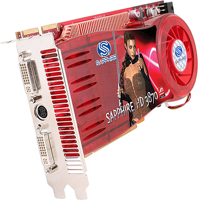
(Image Credit: regmedia.co.uk)
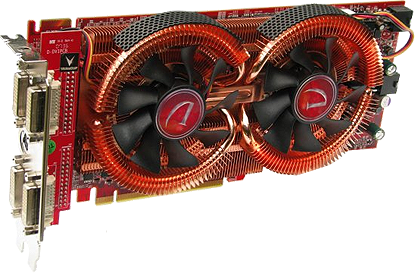
Model: Radeon HD 3870
Date Released: 2007
Interface: PCI-E
Shader Model: 4.1
DirectX: 10.1
Manufacturing Process: 55nm
Core Clockspeed: 775MHz
Memory Clockspeed: 1125MHz
Memory Bus: 256-bit
Transistors: 666 million
(Image Credit: techspot.com)
Model: Radeon HD 3870 X2
Date Released: 2007
Interface: PCI-E
Shader Model: 4.1
DirectX: 10.1
Manufacturing Process: 55nm
Core Clockspeed: 825MHz
Memory Clockspeed: 900MHz
Memory Bus: 256-bit
Transistors: 666 million (x2)
Nvidia GeForce 8 Series
When the G80 was released in 2006, it became the first consumer GPU on the planet to support Windows Vista's Direct3D 10 (D3D10) component. It was a $400 million project in the making and the first brand new architecture from Nvidia in a long time. What made the 8-Series so different from anything Nvidia had done before was the introduction of unified shaders. Prior to this point, pixel shaders and vertex shaders existed as spearate units.
The heavily threaded unified shader architecture proved more efficient than Nvidia's older designs, and it was also considered by some as the "biggest and most complex piece of mass-market silicon ever created." It owed this complexity in part to 681 million transistors at debut, along with support for Shader Model 4.0. The new architecture allowed Nvidia to clock its shader core at a different speed than the rest of the GPU. For example, at launch the 8800 GTX's shader clock ran at 1350MHz, more than twice as fast as the core clockspeed (575MHz).
Once again, Nvidia would release several videocards based on the new series, only this time keeping track of them all would be more confusing than ever. Logic would tell you that performance from top to bottom on the 8800GTS would look like this:
- 8800 GTS 640MB
- 8800 GTS 512MB
- 8800 GTS 320MB
Fun Fact: At roughly 10.5 inches long and weighing 740g, the GeForce 8800 GTX was the largest consumer graphics card ever made. As a result (of the length), many gamers found out that their existing PC case woudn't accomodate the longer videocard, while others had get creative and either bust out the dremel to mod drive cages, or remove a drive cage altogether.
(Image Credit: Foxconn)
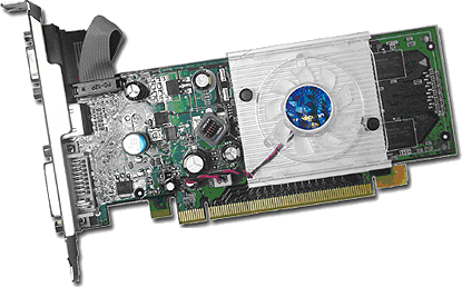
Model: GeForce 8400 GS
Date Released: 2007
Interface: PCI/PCI-E
Shader Model: 4.0
DirectX: 10
Manufacturing Process: 80nm
Core Clockspeed: 450MHz
Memory Clockspeed: 800MHz
Memory Bus: 64-bit
Transistors: 210 million
(Image Credit: tech2.in.com)
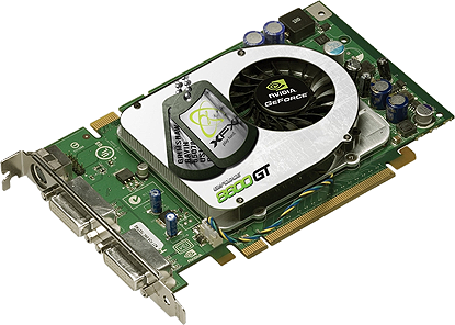
Model: GeForce 8600 GT
Date Released: 2007
Interface: PCI/PCI-E
Shader Model: 4.0
DirectX: 10
Manufacturing Process: 80nm
Core Clockspeed: 540MHz
Memory Clockspeed: 800MHz (DDR2) or 1400MHz (GDDR3)
Memory Bus: 128-bit
Transistors: 289 million
(Image Credit: sysopt.com)
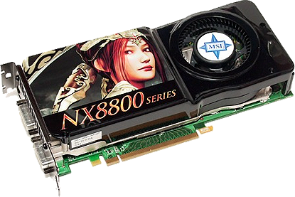
Model: GeForce 8800 GTS (G80)
Date Released: 2007
Interface: PCI-E
Shader Model: 4.0
DirectX: 10
Manufacturing Process: 90nm
Core Clockspeed: 513MHz
Memory Clockspeed: 1584MHz
Memory Bus: 320-bit
Transistors: 681 million
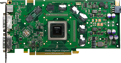
(Image Credit: 3dnews.ru)
Model: GeForce 8800 GTS (G92)
Date Released: 2007
Interface: PCI-E
Shader Model: 4.0
DirectX: 10
Manufacturing Process: 65nm
Core Clockspeed: 650MHz
Memory Clockspeed: 1940MHz
Memory Bus: 256-bit
Transistors: 754 million
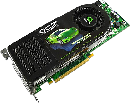
(Image Credit: OCZ)
Model: GeForce 8800 GTX
Date Released: 2006
Interface: PCI-E
Shader Model: 4.0
DirectX: 10
Manufacturing Process: 90nm
Core Clockspeed: 575MHz
Memory Clockspeed: 1800MHz
Memory Bus: 384-bit
Transistors: 484 million
Next, catching up to the present with today's graphical beasts.
Paul has been playing PC games and raking his knuckles on computer hardware since the Commodore 64. He does not have any tattoos, but thinks it would be cool to get one that reads LOAD"*",8,1. In his off time, he rides motorcycles and wrestles alligators (only one of those is true).


