From Voodoo to GeForce: The Awesome History of 3D Graphics
Keep up to date with the most important stories and the best deals, as picked by the PC Gamer team.
You are now subscribed
Your newsletter sign-up was successful
Want to add more newsletters?
Matrox Parhelia
Our condolences go out to you if you happened to be one of the unlucky gamers who spent far too much for a card that performed far too poorly. By all accounts, the Parhelia was supposed to carry Matrox on its shoulders back into the 3D gaming scene after essentially giving up following the G400, and the Parhelia's spec sheet looked hopeful. It had a 256-bit memory bus, was the first to feature a 512-bit ring bus, it came clocked at 220MHz, and a feature called 'Surround Gaming' made it possible to game on three monitors. It even supported DirectX 9, or did it?
Matrox would later admit that the Parhelia's vertex shaders were not DirectX 9-compliant, even though it was advertised as a DX9 videocard. Making matters worse, the Parheila retailed for $400, which meant gamers were paying big bucks for a broken card. And if that weren't enough, cards released by the competition that cost half as much pummeled the Parhelia.
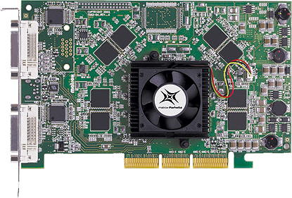
(Image Credit: Matrox)
Model: Parhelia
Date Released: 2002
Interface: PCI-E
Shader Model: 1.1
DirectX: 8
Manufacturing Process: 0.15 micron
Core Clockspeed: 220MHz
Memory Clockspeed: 275MHz
Memory Bus: 256-bit
Transistors: 80 million
ATI Radeon R300
After being leapfrogged by Nvidia, who stole back the performance crown with its GeForce Ti series, it was ATI's turn to jump back in front. The Radeon family entered its third generation in the summer of 2002, which introduced a completely reworked architecture. Even though the R300 was built on the same 0.15-micron manufacturing process, ATI managed to double the number of transistors, ramp up the clockspeeds, and lay claim to having the first fully Direct3D 9-capable desktop graphics card.
Part of the technological leap could be attributed to the use of the flip chip packaging technology. Flipping the die allowed the chip to be more effectively cooled, opening up additional frequency headroom that otherwise wouldn't have been attainable. But higher clockspeeds wasn't the only thing the R300 had going for it. This was the first time a graphics chip maker put out a product that fully utilized a 256-bit bus (let's not even revisit the Parhelia). Along with an integrated crossbar memory controller, the R300 excelled at memory intensive tasks.
ATI had again regained the top benchmark spots with its 9700 Pro, and later the 9800 Pro and XT. Several other videocards would flesh out the then modern Radeon lineup.
Keep up to date with the most important stories and the best deals, as picked by the PC Gamer team.
Fun Fact: Budget buyers found a gem in the 9500 Pro, which some enthusiasts were able to mod into a 9700 non-Pro. Even when unsuccessful, the 9500 Pro proved popular because of its 8 pixel pipelines and resulting fast performance.
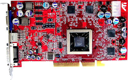
(Image Credit: comresurs.ru)
Model: Radeon 9500 Pro
Date Released: 2002
Interface: AGP
Shader Model: 2.0
DirectX: 9
Manufacturing Process: 0.15 micron
Core Clockspeed: 275MHz
Memory Clockspeed: 270MHz
Memory Bus: 128-bit
Transistors: 107 million
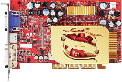
(Image Credit: techspot.com)
Model: Radeon 9700 Pro
Date Released: 2002
Interface: AGP
Shader Model: 2.0
DirectX: 9
Manufacturing Process: 0.15 micron
Core Clockspeed: 325MHz
Memory Clockspeed: 310MHz
Memory Bus: 256-bit
Transistors: 107 million
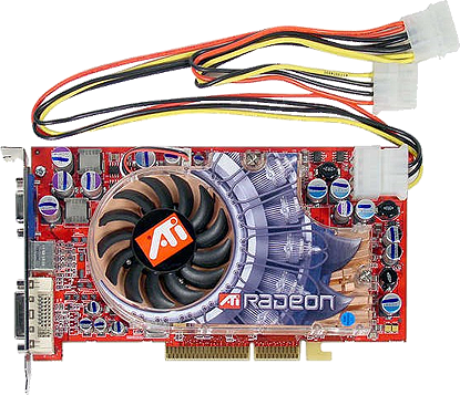
(Image Credit: foroswebgratis.com)
Model: Radeon 9800 XT
Date Released: 2003
Interface: AGP
Shader Model: 2.0
DirectX: 9
Manufacturing Process: 0.15 micron
Core Clockspeed: 380MHz
Memory Clockspeed: 350MHz
Memory Bus: 256-bit
Transistors: 107 million
Nvidia GeForce FX Series
Whereas the GeForce 4 was, for all intents and purposes, a revised GeForce 3, Nvidia opted to change its naming scheme for its fifth generation of GeForce cards calling it the FX Series. This also gave birth to the infamous Dawn fairy and the accompanying demo designed to show off what the new architecture was capable of.
One such feature was support for Shader Model 2.0, a requirement of the then-recently released DirectX 9 API. Nvidia's FX Series were the company's first videocards to support SM2.0. Depending on the model, FX cards made use of DDR, DDR2, or GDDR3 memory and a 0.13 micron manufacturing process.
Fun Fact: The FX5800's two-slot cooling solution drew heavy criticism over its excessive noise. It was so loud, many likened it to a dustbuster, and it didn't help that it looked a little bit like one.
Fun Fact 2: Soon after the Dawn demo was released, it was hacked by the online community to work with any ATI card that supported DirectX 9. The modified demo file also featured a naughty NSFW mode when users renamed the executable 3dmark03.exe or quake3.exe.
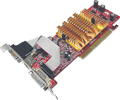
(Image Credit: Directron)
Model: GeForce FX 5200
Date Released: 2003
Interface: AGP/PCI
Shader Model: 2.1
DirectX: 9
Manufacturing Process: 0.15 micron
Core Clockspeed: 250MHz
Memory Clockspeed: 400MHz
Memory Bus: 64- and 128-bit
Transistors: 45 million
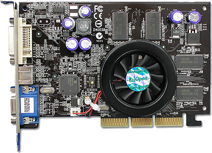
(Image Credit: AOpen)
Model: GeForce FX 5600
Date Released: 2003
Interface: AGP
Shader Model: 2.1
DirectX: 9
Manufacturing Process: 0.13 micron
Core Clockspeed: 350MHz
Memory Clockspeed: 700MHz
Memory Bus: 128-bit
Transistors: 80 million
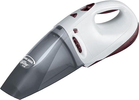
Model: GeForce FX 5800
Date Released: 2003
Interface: AGP
Shader Model: 2.1
DirectX: 9
Manufacturing Process: 0.13 micron
Core Clockspeed: 400MHz
Memory Clockspeed: 800MHz
Memory Bus: 128-bit
Transistors: 15 million
ATI Radeon R420
Unlike the jump from R200 to R300, ATI didn't totally revamp the core architecture to come up with R420. What the chip maker did do was introduce a new design process, in which R420 cards were manufactured with 0.13-micron low-k dielectric technology. We won't bore you (or ourselves) with all the technical details - in short, ATI was able to produce higher frequency cards that consumed less power and ran cooler. That's a win-win proposition.
In order to maximize its manufacturing potential, the R420 arranged its pixel pipelines into groups of four. If a quad proved defective, ATI could disable it and still sell chipsets with 12, 8, or 4 pipelines for different market sectors.
Introduced with the new architecture was a new naming scheme, starting with the X800 XT Platinum, X800 Pro, and X800 SE. These three cards came configured with 16, 12, and 8 pixel pipelines, respectively, the latter two sporting one and two disabled quads.
Fun Fact: The first generation of CrossFire cards appeared in 2005, but it wasn't as elegant as it is today. Gamers couldn't just toss any two videocards into their system; instead, one had to be a 'Master' version, which would connect to the other card via a DVI Y- dongle.
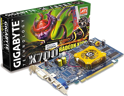
(Image Credit: Gigabyte)
Model: Radeon X700
Date Released: 2004
Interface: AGP/PCI-E
Shader Model: 2.0
DirectX: 9
Manufacturing Process: 0.11 micron
Core Clockspeed: 400MHz
Memory Clockspeed: 350MHz
Memory Bus: 128-bit
Transistors: 120 million
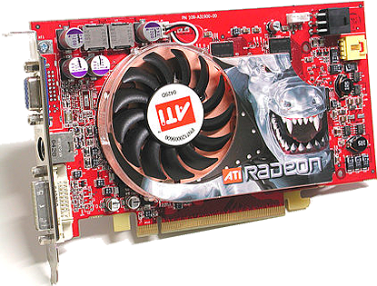
(Image Credit: thg.ru)
Model: Radeon X800 XT Platinum
Date Released: 2004
Interface: AGP/PCI-E
Shader Model: 2.0
DirectX: 9
Manufacturing Process: 0.13 micron
Core Clockspeed: 520MHz
Memory Clockspeed: 540MHz
Memory Bus: 256-bit
Transistors: 120 million
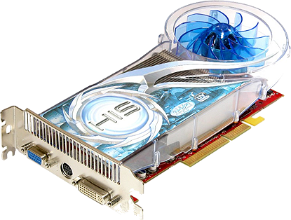
(Image Credit: tecnacom.nl)
Model: Radeon X850 XT Platinum
Date Released: 2004
Interface: AGP/PCI-E
Shader Model: 2.0
DirectX: 9
Manufacturing Process: 0.13 micron
Core Clockspeed: 540MHz
Memory Clockspeed: 590MHz
Memory Bus: 256-bit
Transistors: 160 million
Next, like Star Trek movies, Nvidia's even-series cards deliver again.
Paul has been playing PC games and raking his knuckles on computer hardware since the Commodore 64. He does not have any tattoos, but thinks it would be cool to get one that reads LOAD"*",8,1. In his off time, he rides motorcycles and wrestles alligators (only one of those is true).


