From Voodoo to GeForce: The Awesome History of 3D Graphics
Keep up to date with the most important stories and the best deals, as picked by the PC Gamer team.
You are now subscribed
Your newsletter sign-up was successful
Want to add more newsletters?
Nvidia GeForce 9 Series
A new series does not a new architecture make, and that's certainly the case with Nvidia's ninth generation of GeForce parts. In fact, the G92 core (notice the '9') had already found its way onto thousands of desktops before the 9-series was ever introduced. We're of course referring to the G92-based 8800 GTS 512MB discussed earlier. So what exactly was going on?
For the first time in a long time, nothing much was going on. AMD didn't seem interested (or capable) in competing at the high end, leading to a lull in the graphics wars. Whether or not this influenced Nvidia's roadmap is debatable, but rather than release a new architecture, many considered the 9-Series little more than a rebranding of existing parts. And in many ways, it was. If we're to compare the new with the old, both the 9800 GTX and G92-based 8800 GTS contain 128 stream processors, 16 ROPs, are built on a 65nm manufacturing process, have a 256-bit memory bus, and pack 754 transistors.
Kicking off the 9-Series, however, was the G94-based 9600 GT. Despite the higher number, the G94 has only half the number of stream processors as the G92 (64 versus 128), and still less than the 112 found on the 8800 GT. It also has 33 percent fewer transistors than the G92.
Article continues below 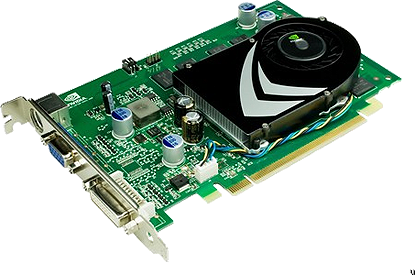
(Image Credit: Nvidia)
Model: GeForce 9400 GT
Date Released: 2008
Interface: PCI-E
Shader Model: 4.0
DirectX: 10
Manufacturing Process: 55nm
Core Clockspeed: 550MHz
Memory Clockspeed: 800MHz
Memory Bus: 128-bit
Transistors: 314 million
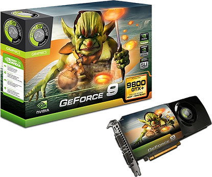
(Image Credit: hardware.info)
Model: GeForce 9800 GTX+
Date Released: 2008
Interface: PCI-E
Shader Model: 4.0
DirectX: 10
Manufacturing Process: 55nm
Core Clockspeed: 738MHz
Memory Clockspeed: 2200
Memory Bus: 256-bit
Transistors: 754 million
Keep up to date with the most important stories and the best deals, as picked by the PC Gamer team.
ATI Radeon R700
Announced in 2008, the R700 chipset made it possible for ATI to once again compete at the high end, when it had previously been focusing almost exclusively on the mid-range and entry-level markets. A few key architectural changes made this move up the performance ladder possible, or maybe better it would better to refer to them as architectural refinements, as the overall design remains similar to the R600/R670.
ATI reworked the tesselation unit in R700 so that it could now export data to the geometry shader, allowing the two to work together, and do so efficiently. ROPs have been completely rebuilt for speed in R700 and sport dedicated hardware-based multi-sampled AA resolve. The result is a much less dramatic fall-off in performance when AA is cranked up. And with the RV770 revision, ATI's GPUs became the first to support GDDR5 memory.
Related to the new architecture, ATI just recently released the HD 4890, the fastest R7xx-based single-GPU videocard in the company's lineup. The dual -GPU 4870X2 remains the company's flaghips model, and is much more readily available than Nvidia's GTX 295.
Fun Fact: At the end of March 2009, AMD made available a 392-page PDF reference guide on its R700-family Instruction Set Architecture. The 1.88MB document is intended for programmers writing appls and system software, and you can download it here .
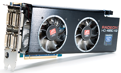
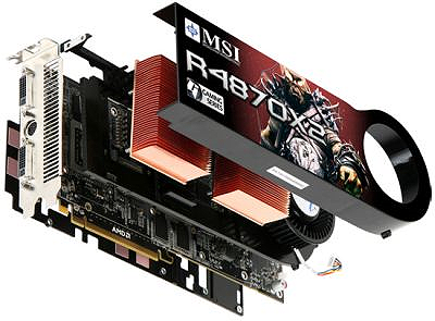
Model: Radeon HD 4850 X2
Date Released: 2008
Interface: PCI-E
Shader Model: 4.1
DirectX: 10.1
Manufacturing Process: 55nm
Core Clockspeed: 650MHz
Memory Clockspeed: 993MHz
Memory Bus: 256-bit
Transistors: 956 million (x2)
(Image Credit: geeks3d.com)
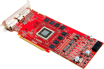
Model: Radeon HD 4870 X2
Date Released: 2008
Interface: PCI-E
Shader Model: 4.1
DirectX: 10.1
Manufacturing Process: 55nm
Core Clockspeed: 750MHz
Memory Clockspeed: 900MHz
Memory Bus: 256-bit
Transistors: 956 million (x2)
(Image Credit: HotHardware)
Model: Radeon HD 4890
Date Released: 2009
Interface: PCI-E
Shader Model: 4.1
DirectX: 10.1
Manufacturing Process: 55nm
Core Clockspeed: 850MHz
Memory Clockspeed: 900MHz
Memory Bus: 256-bit
Transistors: 960 million
Nvidia GeForce G 100 Series
If you managed to miss the release of Nvidia's G 100 Series, don't sweat it. No big PR fanfare would accompany the 'new' cards, which aren't really new at all. Instead, the G 100 nomenclature was designed to replace the 9-Series in the OEM market. Minus a few clockspeed adjustments here and there, nothing separated one Series from the other.
Nvidia GeForce 200 Series
Continuing with the unified shader architecture that has served Nvidia well since the 8-Series, the latest chipset pushes the design envelope by stuffing 1.4 billion transistors into the GPU. Let's say that again: 1.4 BILLION transistors. This translates into 930 gigaFLOPs of processing power for the GTX 280, which launched alongside the GTX 260 when Nvidia introduced the updated architecture.
More than just a simple rehash of the 8- and 9-Series GPUs, the 200 series added considerable muscle by outfitting the GTX 280 with 240 stream processors, nearly twice as many as the fastest 9800 videcoard, and 192 stream processors on the GTX 260. These were both built on a 65nm manufacturing process, however Nvidia has since switched to 55nm, and as part of that, has released the GTX 260. This newer revision is identifiable by its Core 216 designation, which refers to the number of shader processors, up from 192 on the original.
While Nvidia didn't re-release the GTX 280, it did add the 285 to its lineup, currently the fastest single-GPU card in the entire lineup. Serving as the flagship part, Nvidia's GTX 295 packs two GPUs into a single board, which again is comprised of two PCBs sandwiched together. As of this writing, the GTX 295 ranks as the fastest videocard in the universe with a mind boggling 1,788 gigaFLOPs of processing power.
Fun Fact: While feuding with Intel over a Nehalem licensing agreement, Nvidia CEO Jen-Hsun Huang said the "the CPU has run its course and the soul of the PC is shifting quickly to the GPU," a notion which refers to general purpose computing on the GPU (GPGPU). He went on to call the CPU a "decaying" business.
(Image Credit: hothardware.com)
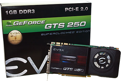
Model: GeForce GTS 250 (G92)
Date Released: 2009
Interface: PCI-E
Shader Model: 4.0
DirectX: 10
Manufacturing Process: 65nm and 55nm
Core Clockspeed: 738MHz
Memory Clockspeed: 2200MHz
Memory Bus: 256-bit
Transistors: 754 million
(Image Credit: gearlog.com)
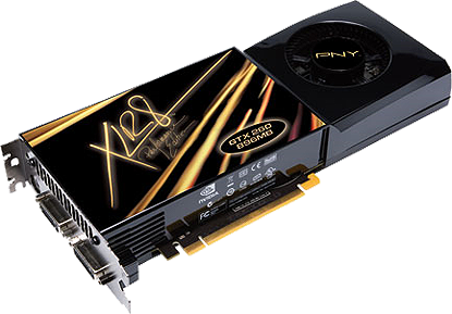
Model: GeForce GTX 260
Date Released: 2008
Interface: PCI-E
Shader Model: 4.0
DirectX: 10
Manufacturing Process: 65nm and 55nm
Core Clockspeed: 576MHz
Memory Clockspeed: 1998MHz
Memory Bus: 448-bit
Transistors: 1400 million
(Image Credit: Nvidia)
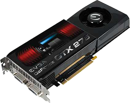
Model: GeForce GTX 275
Date Released: 2009
Interface: PCI-E
Shader Model: 4.0
DirectX: 10
Manufacturing Process: 55nm
Core Clockspeed: 633MHz
Memory Clockspeed: 2268MHz
Memory Bus: 448-bit
Transistors: 1400 million
(Image Credit: gameguru.in)
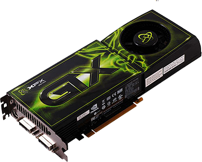
Model: GeForce GTX 280
Date Released: 2008
Interface: PCI-E
Shader Model: 4.0
DirectX: 10
Manufacturing Process: 55nm
Core Clockspeed: 602MHz
Memory Clockspeed: 2214MHz
Memory Bus: 512-bit
Transistors: 1400 million
(Image Credit: bit-tech.net)
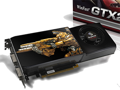
Model: GeForce GTX 285
Date Released: 2009
Interface: PCI-E
Shader Model: 4.0
DirectX: 10
Manufacturing Process: 55nm
Core Clockspeed: 648MHz
Memory Clockspeed: 2484MHz
Memory Bus: 512-bit
Transistors: 1400 million
(Image Credit: hardware.info)
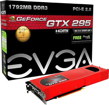
Model: GeForce GTX 295
Date Released: 2009
Interface: PCI-E
Shader Model: 4.0
DirectX: 10
Manufacturing Process: 55nm
Core Clockspeed: 576MHz
Memory Clockspeed: 1998MHz
Memory Bus: 448-bit
Transistors: 1400 million
Paul has been playing PC games and raking his knuckles on computer hardware since the Commodore 64. He does not have any tattoos, but thinks it would be cool to get one that reads LOAD"*",8,1. In his off time, he rides motorcycles and wrestles alligators (only one of those is true).


