AMD Vega: Everything you need to know about the next GPU architecture
How AMD's next GPU may outperform the GTX 1080 or even the Titan X.
At AMD's Tech Summit in December, press, partners, and analysts were briefed on some of AMD's upcoming products; today we can finally talk about everything we saw. I've already talked a lot about Zen/Ryzen, but for gamers the bigger news is Vega. AMD gave us a roadmap last year listing their plans for GPU architectures: first Polaris, then Vega, and after that Navi. Polaris targeted the mainstream gaming audience, with good performance and efficiency, but Vega sets its sights higher, with a release target of "first half, 2017"—probably June, judging by AMD's past history.
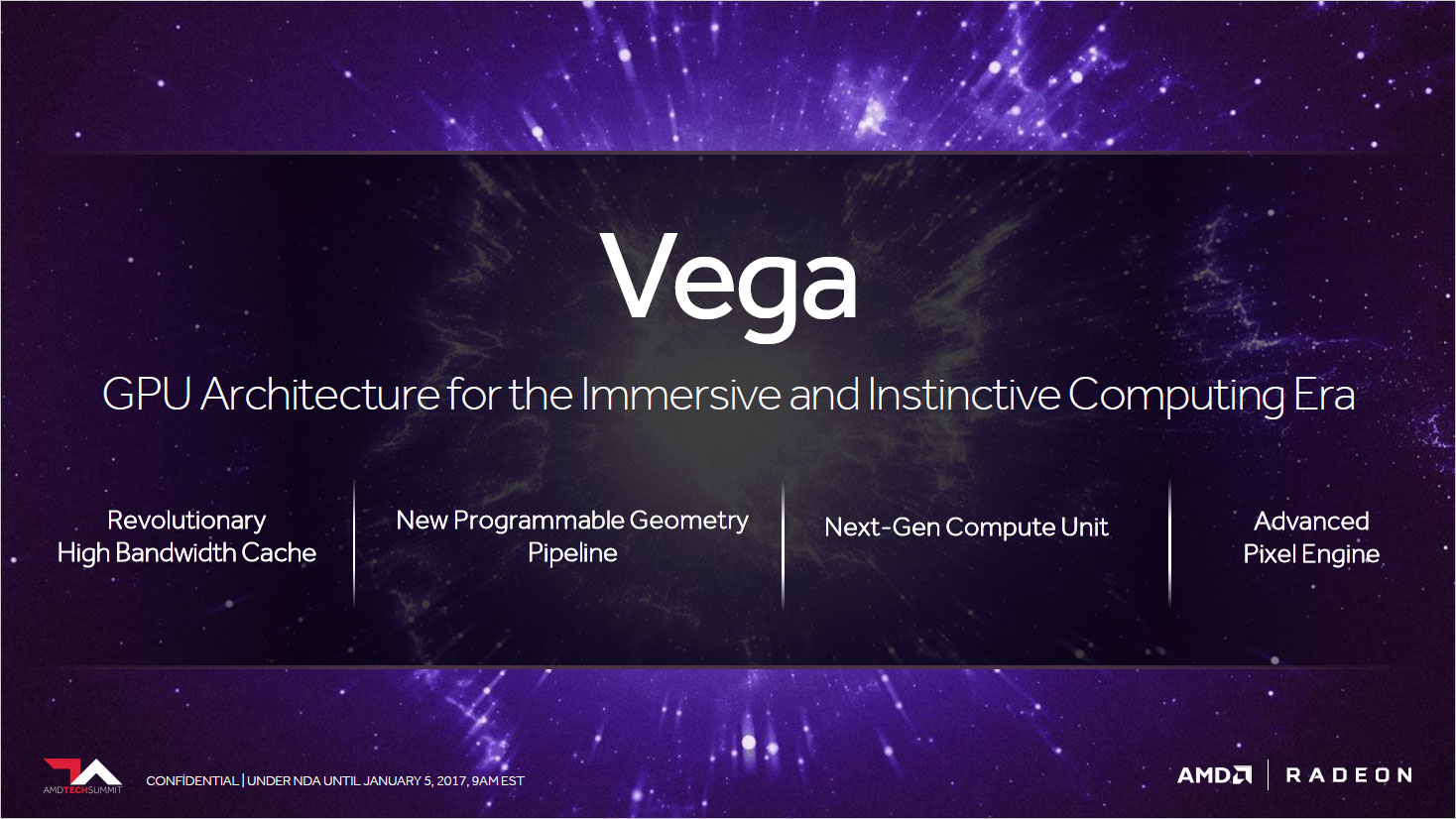
Along with working silicon, AMD has now released the first official details on Vega, and it's shaping up to be, *ahem*, out of this world.
Vega builds on everything that makes Polaris great, but it's not simply a bigger chip with more cores. AMD didn't provide Vega's core count or clock speed, but it will likely be 4,096 cores clocked at around 1.5-1.6GHz. The reason I can be so specific is that AMD also announced a new line of machine intelligence accelerators, called Radeon Instinct MI6, MI8, and MI25. The MI25 uses Vega and will provide up to 25 TFLOPS (with FP16—half that for FP32), which means the baseline for Vega is about 45 percent faster than the Fury X. Chew on that for a minute—45 percent faster than Fury X should put it well above the performance level of the GTX 1080, possibly even eclipsing the Titan X (and thereby the 1080 Ti).

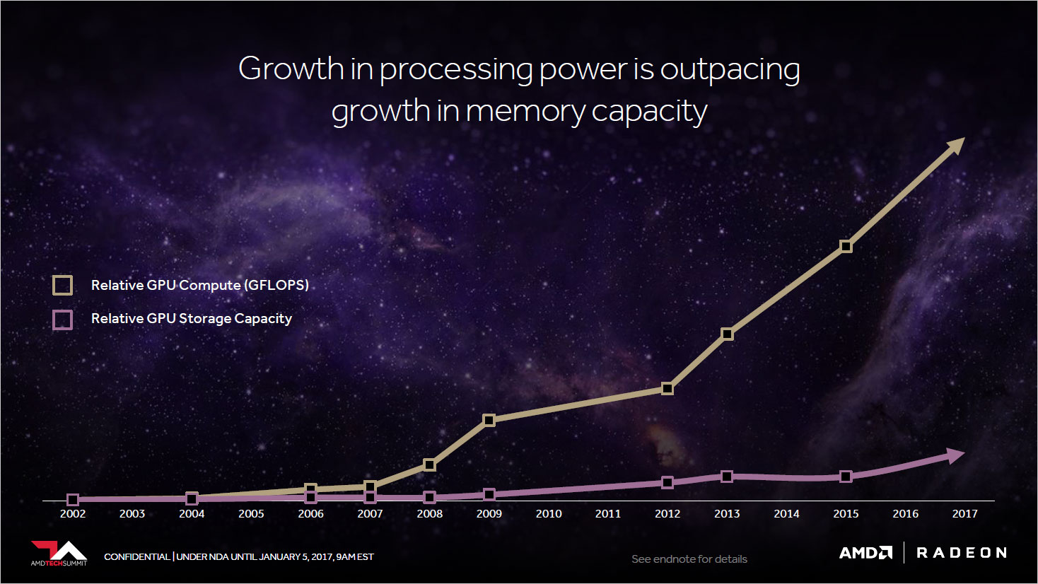
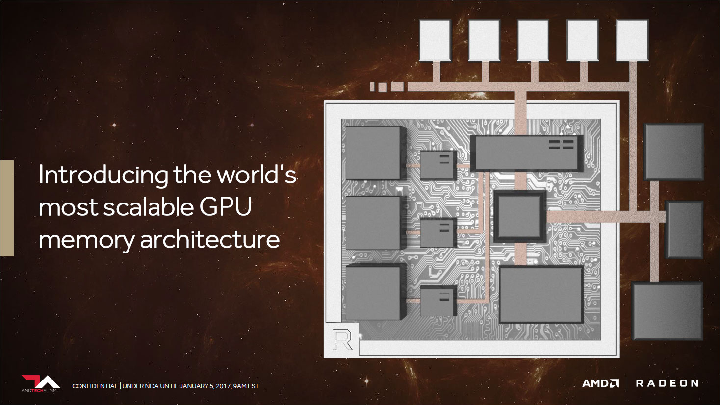
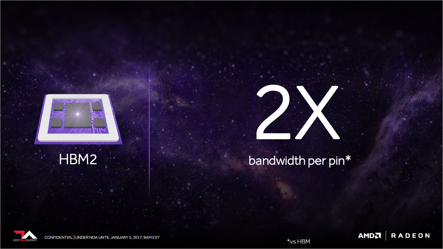
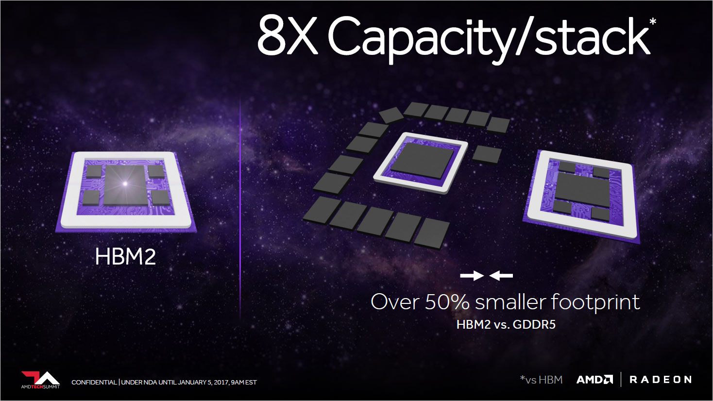
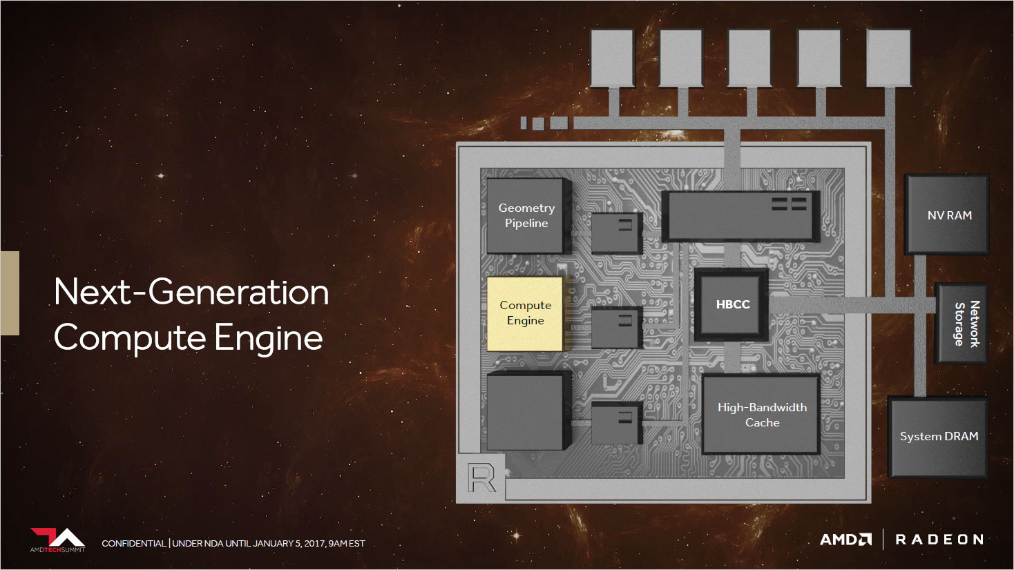
It's not just about TFLOPS, however. AMD has reworked several key elements of their GCN architecture, a major one being the memory subsystem. Vega includes 8GB (possibly 16GB) of HBM2 memory in two stacks. These deliver the same 512GB/s bandwidth as the four stacks of HBM1 in Fiji, but with two stacks the silicon interposer doesn't need to be as large, and HBM2 densities allow AMD to double (potentially quadruple) the amount of memory. We've seen quite a few instances where 4GB can limit performance, so Vega takes care of that problem.

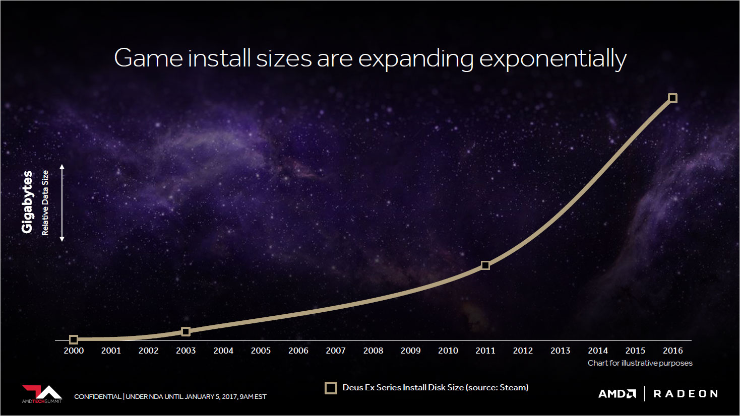
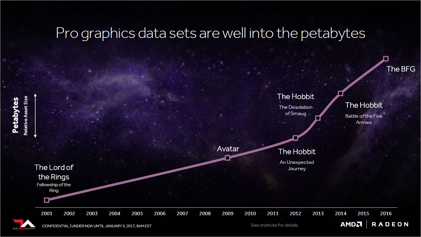
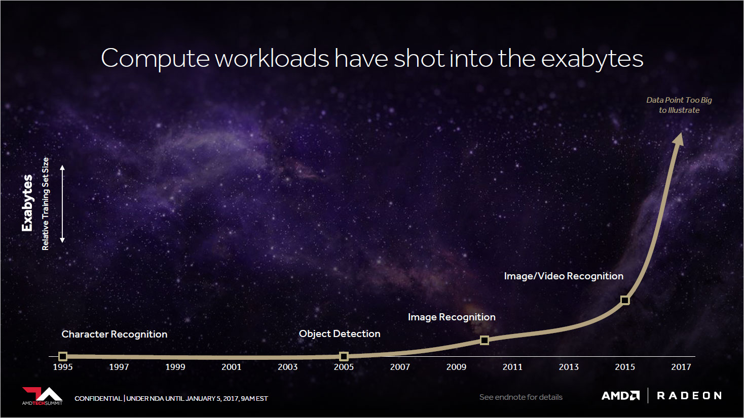
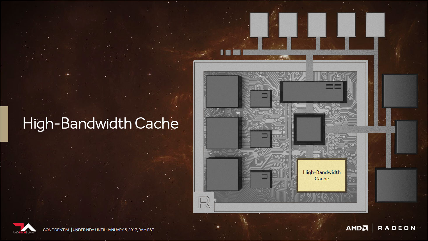
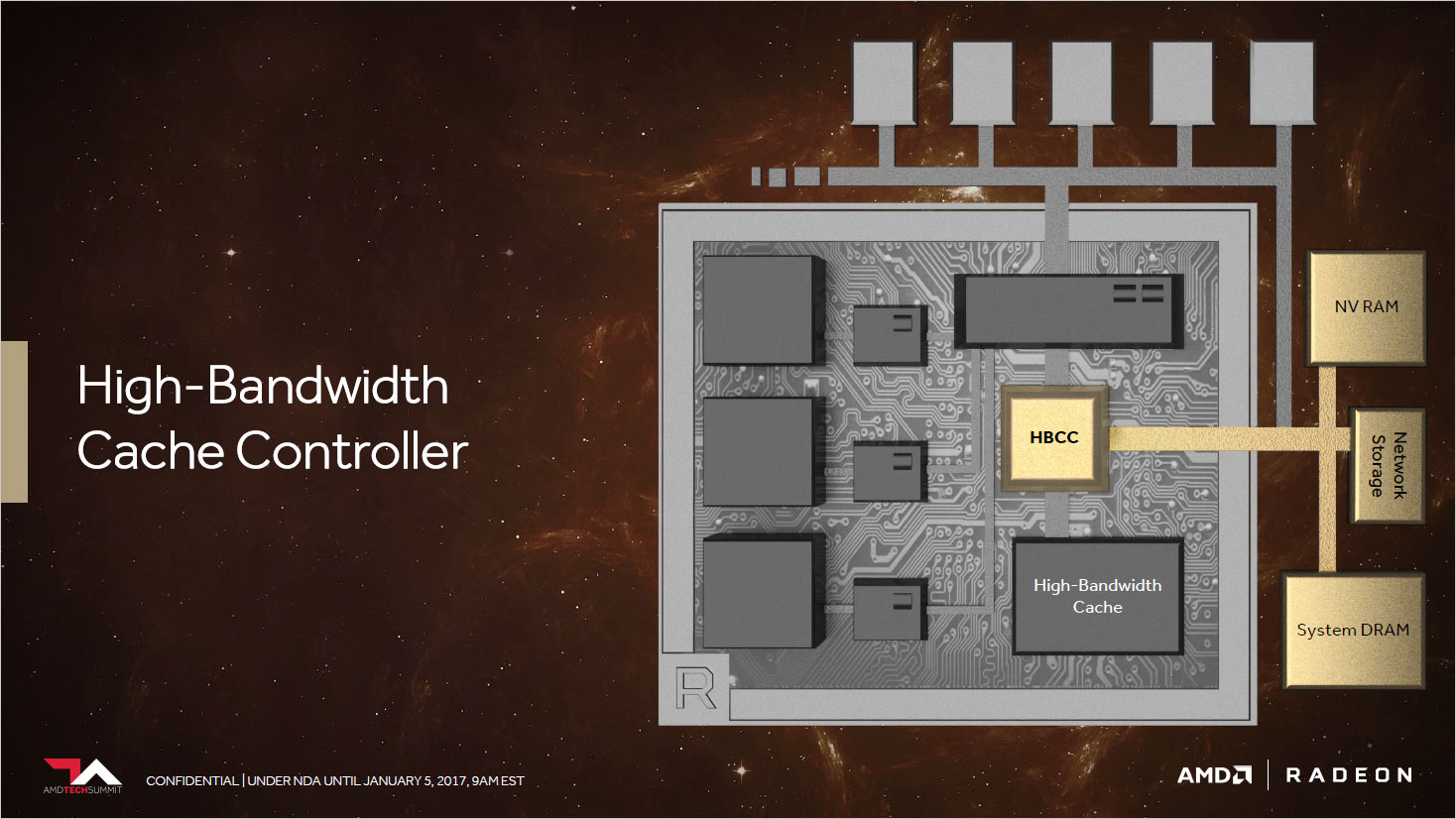
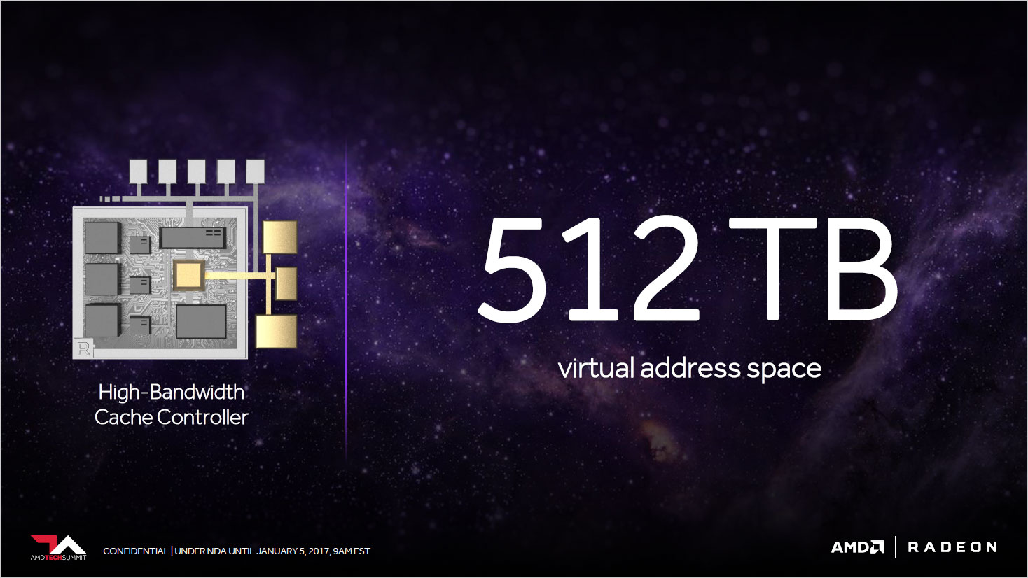
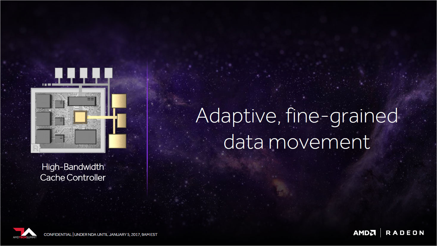
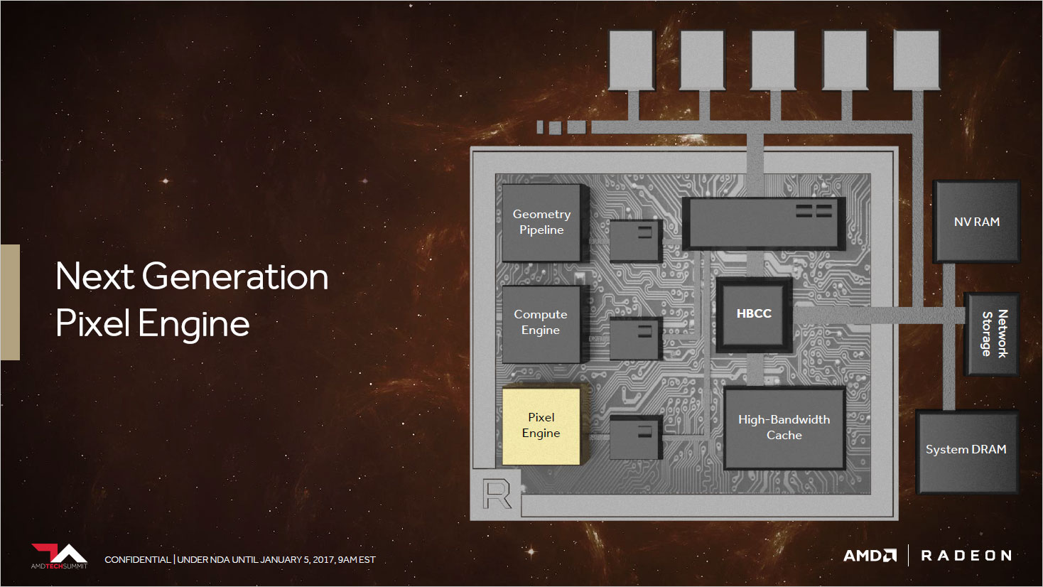
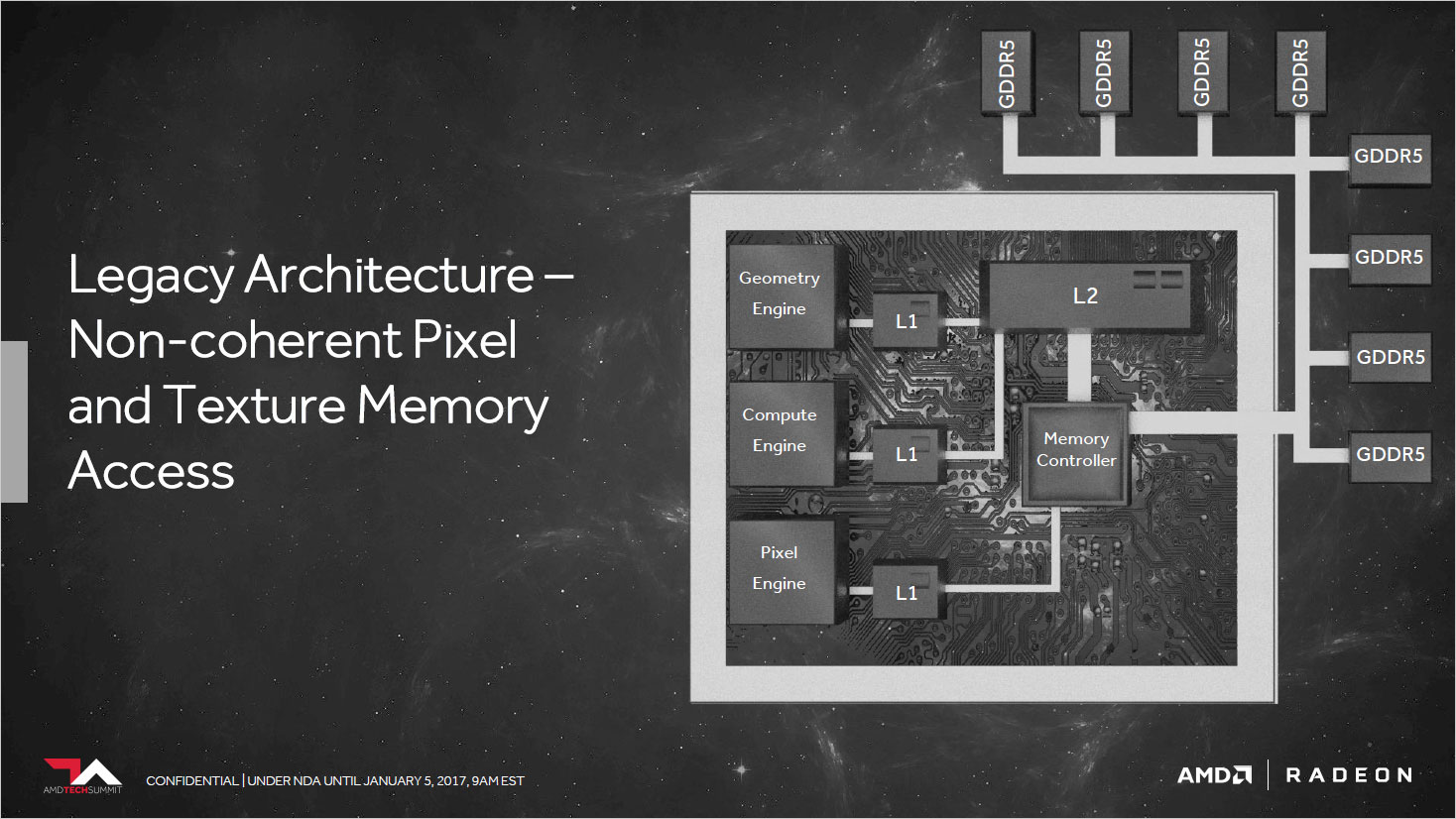
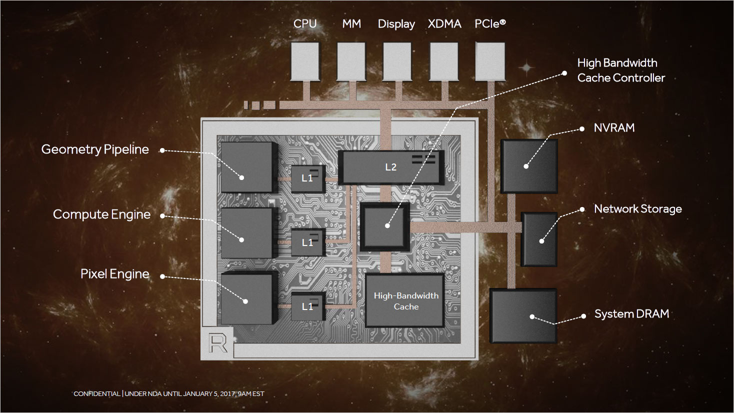
But AMD isn't just calling this HBM or VRAM; it's now a "High-Bandwidth Cache" (HBC) and there's also a new "High-Bandwidth Cache Controller" (HBCC). The distinction is important, because the HBCC plays a much more prominent role in memory accesses. AMD calls this a "completely new memory hierarchy." That's probably a bit of hyperbole, but the idea is to better enable the GPU to work with large data sets, which is becoming an increasingly difficult problem.
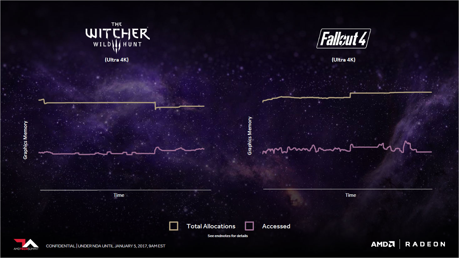
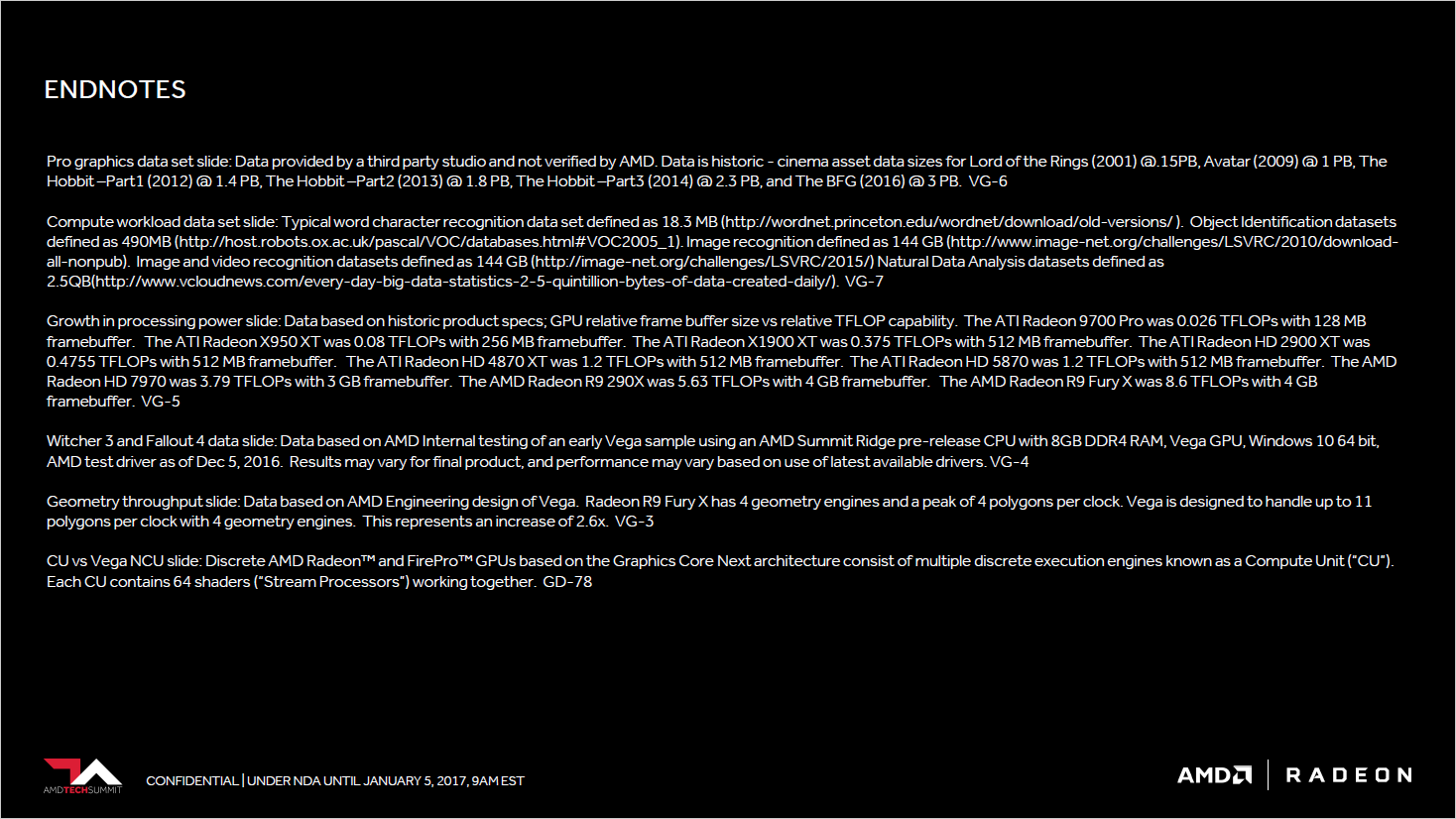
As an example of why the HBCC is important, AMD profiled VRAM use for The Witcher 3 and Fallout 4. In both cases, the amount of VRAM allocated is around 2-3 times larger than the amount of VRAM actually 'touched' (accessed) during gameplay. The HBCC takes this into account, allowing the GPU to potentially work with significantly larger data sets, providing a 512TB virtual address space.
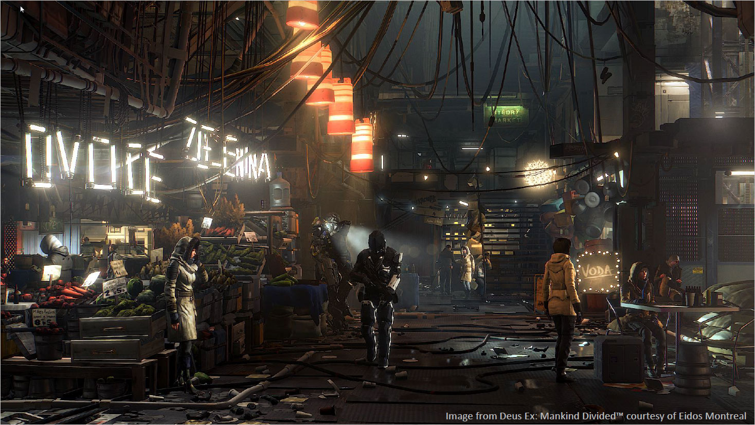
AMD also demonstrated a real-time physically rendered image of a house using more than 600GB of data, running on what I assume is an 8GB Vega card. If the HBCC works as AMD claims, even a 8GB card could potentially behave more like an 16-24GB VRAM card, while a 16GB card would equal a 32-48GB card.
The biggest gaming news, reviews and hardware deals
Keep up to date with the most important stories and the best deals, as picked by the PC Gamer team.

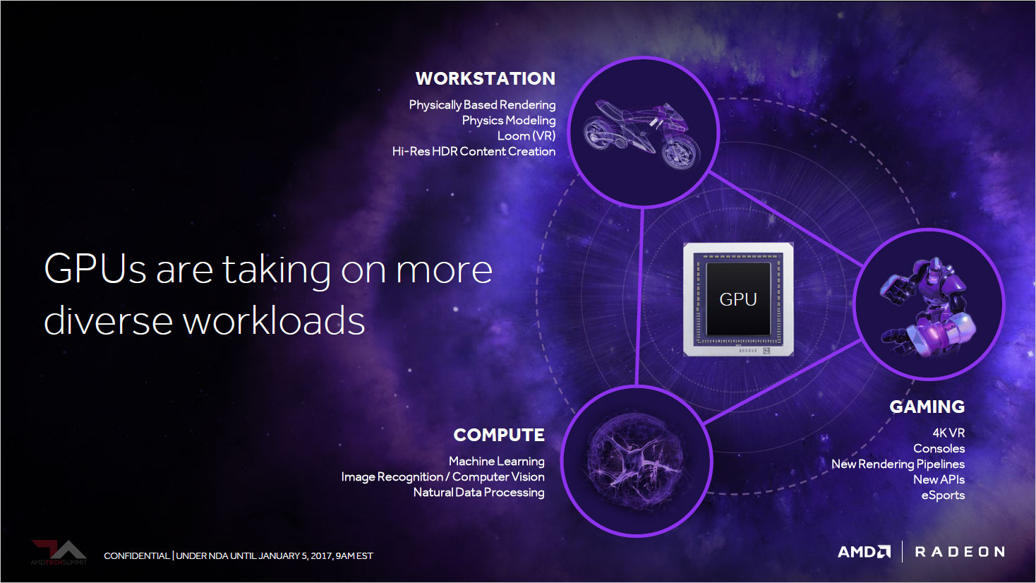
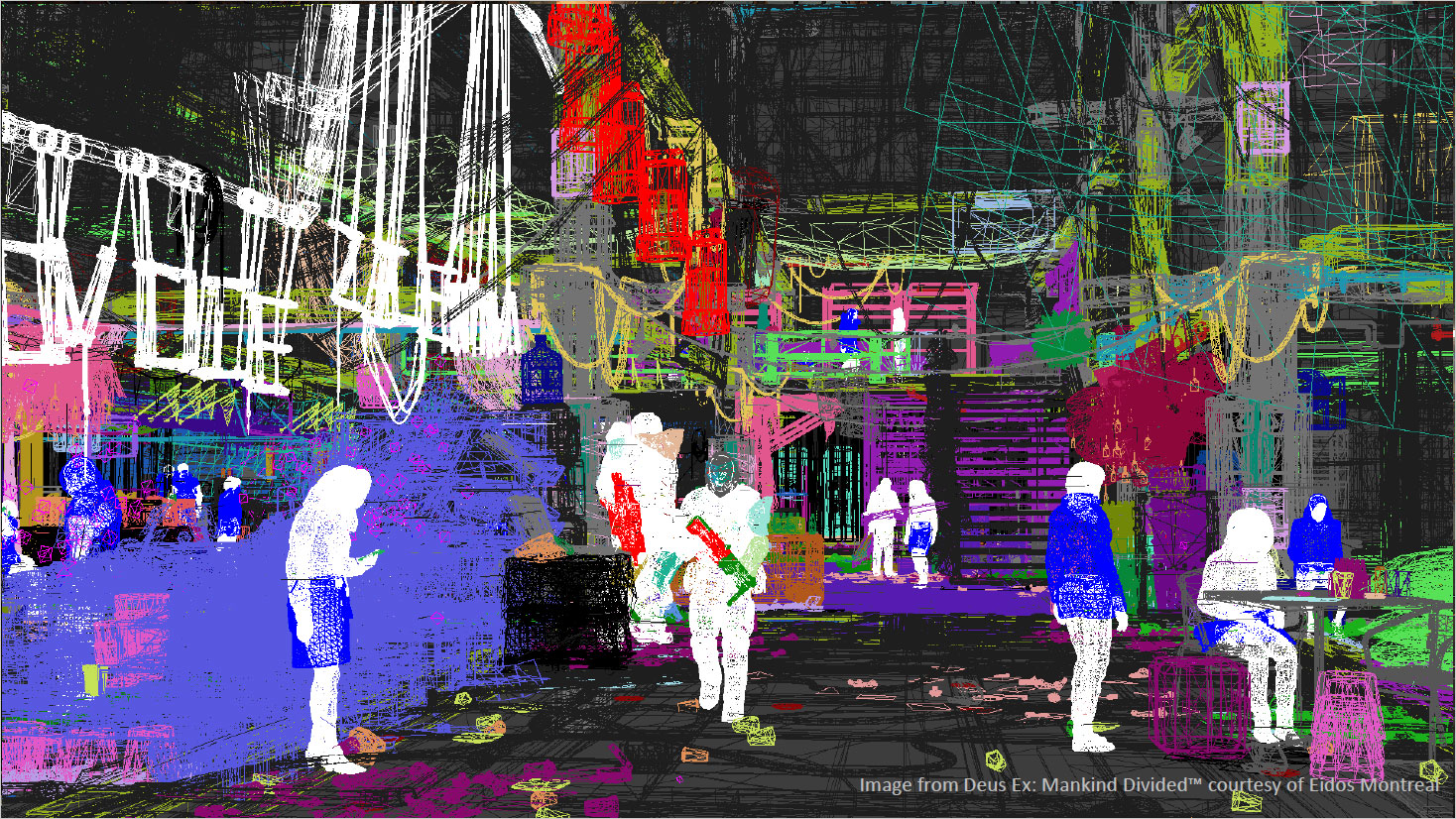
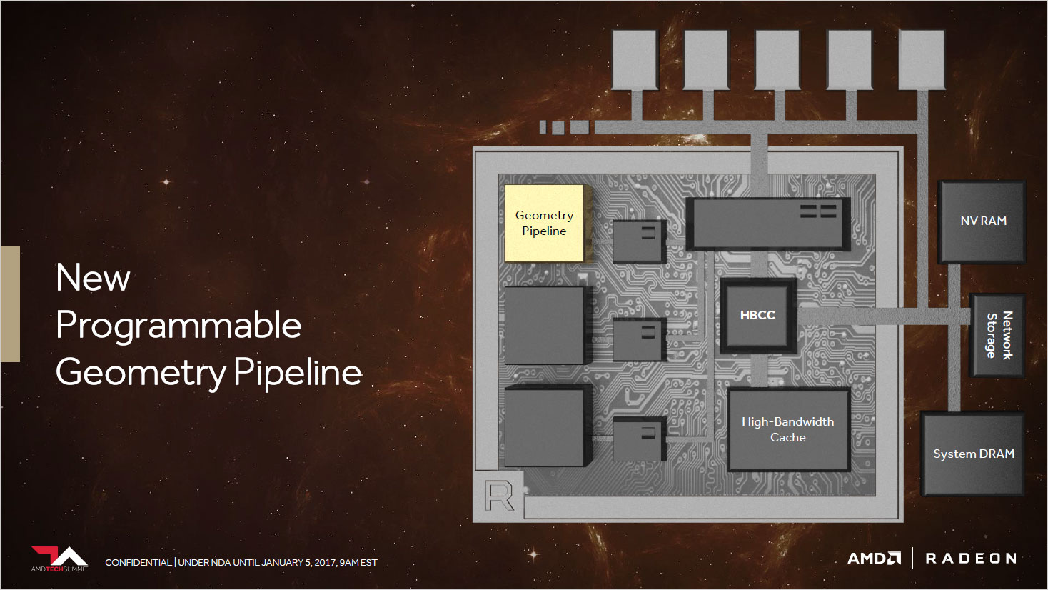
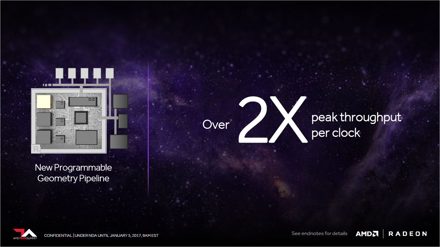
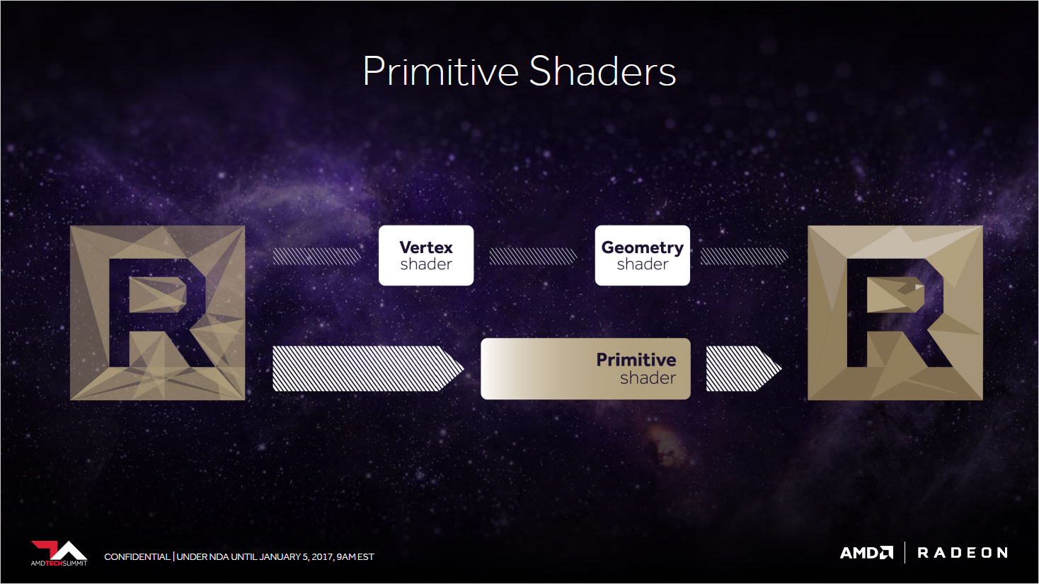
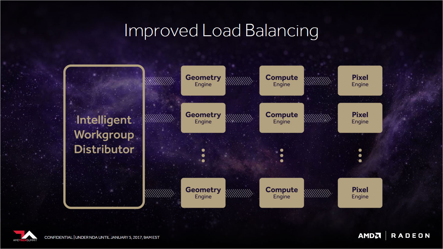
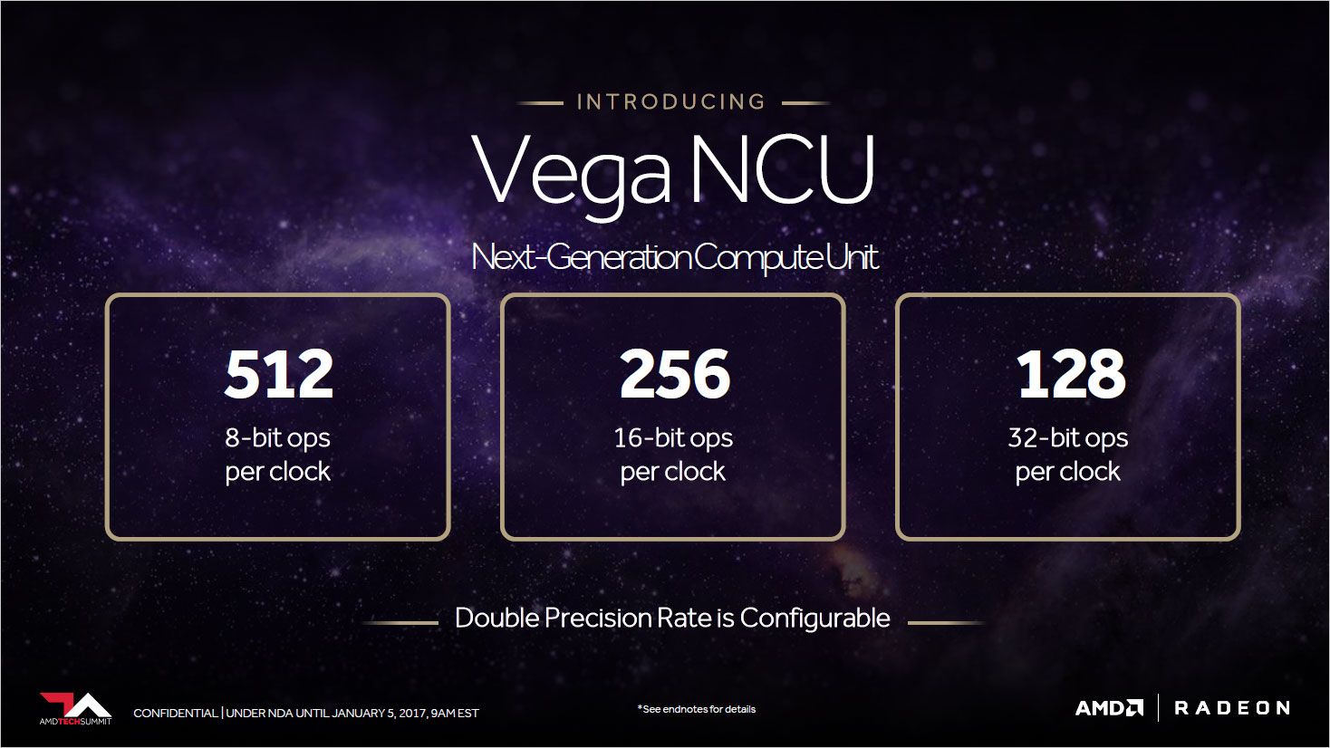
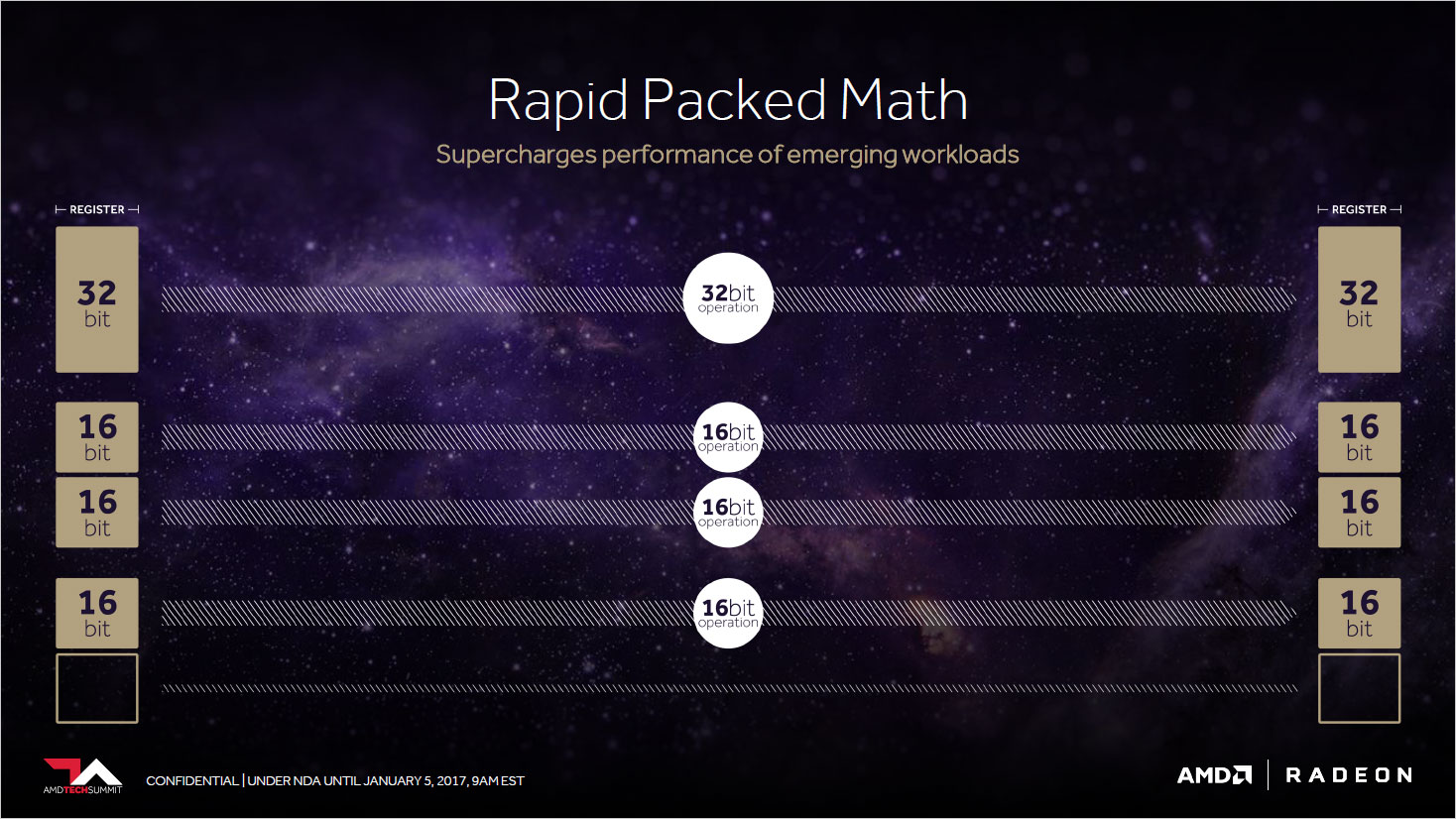
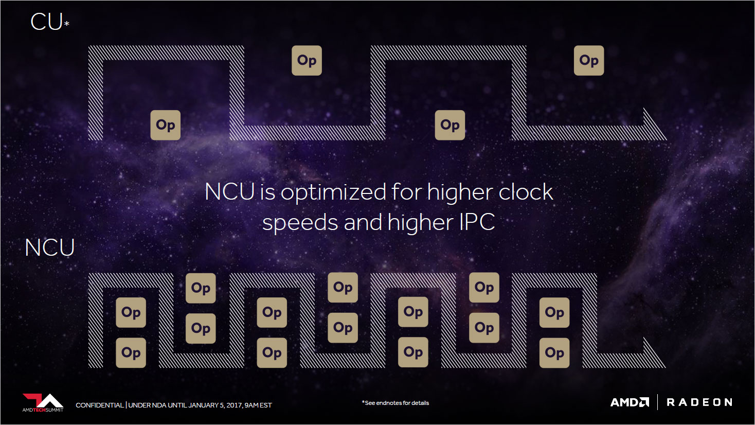
Vega also has a new geometry pipeline. Similar to the VRAM use, AMD notes that there can be a 100X difference between polygons in a scene and those that are visible on the screen. To help, the new geometry engine will have over twice the throughput per clock compared to AMD's previous architecture. The compute unit is also improved, with native support for packed FP16 operations, which should prove very useful for machine learning applications. AMD's Mike Mantor also stated, "We've spent a lot of time tuning and tweaking to get our frequencies up—significantly—and power down," though note that the Radeon Instinct MI25 still has a "<300W" TDP.
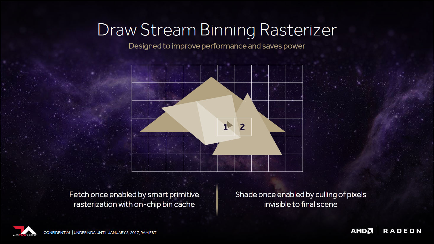

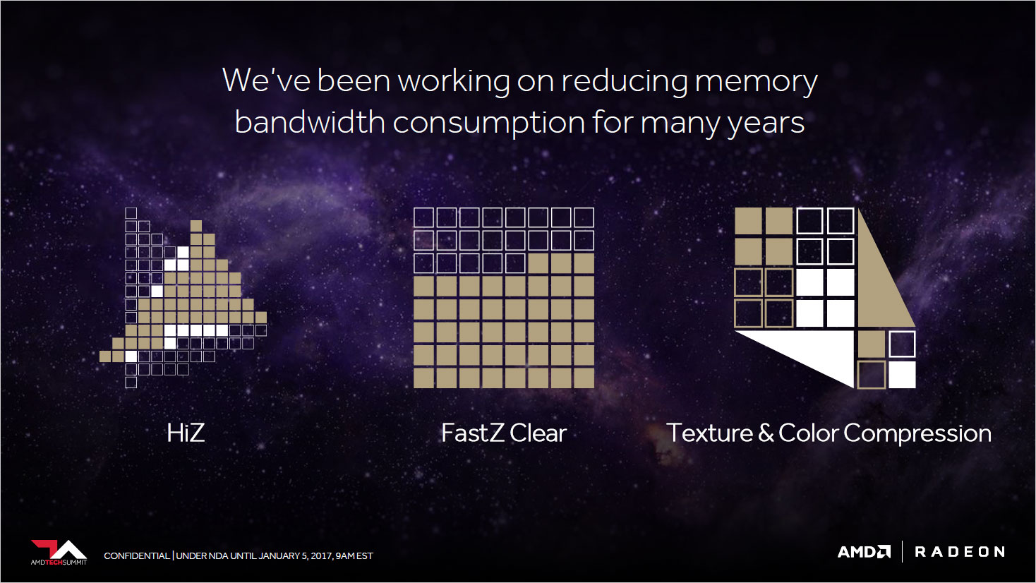
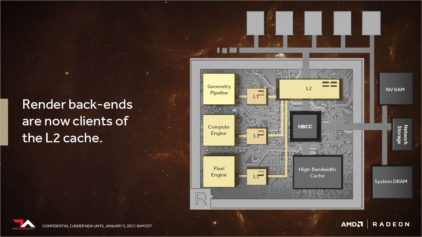
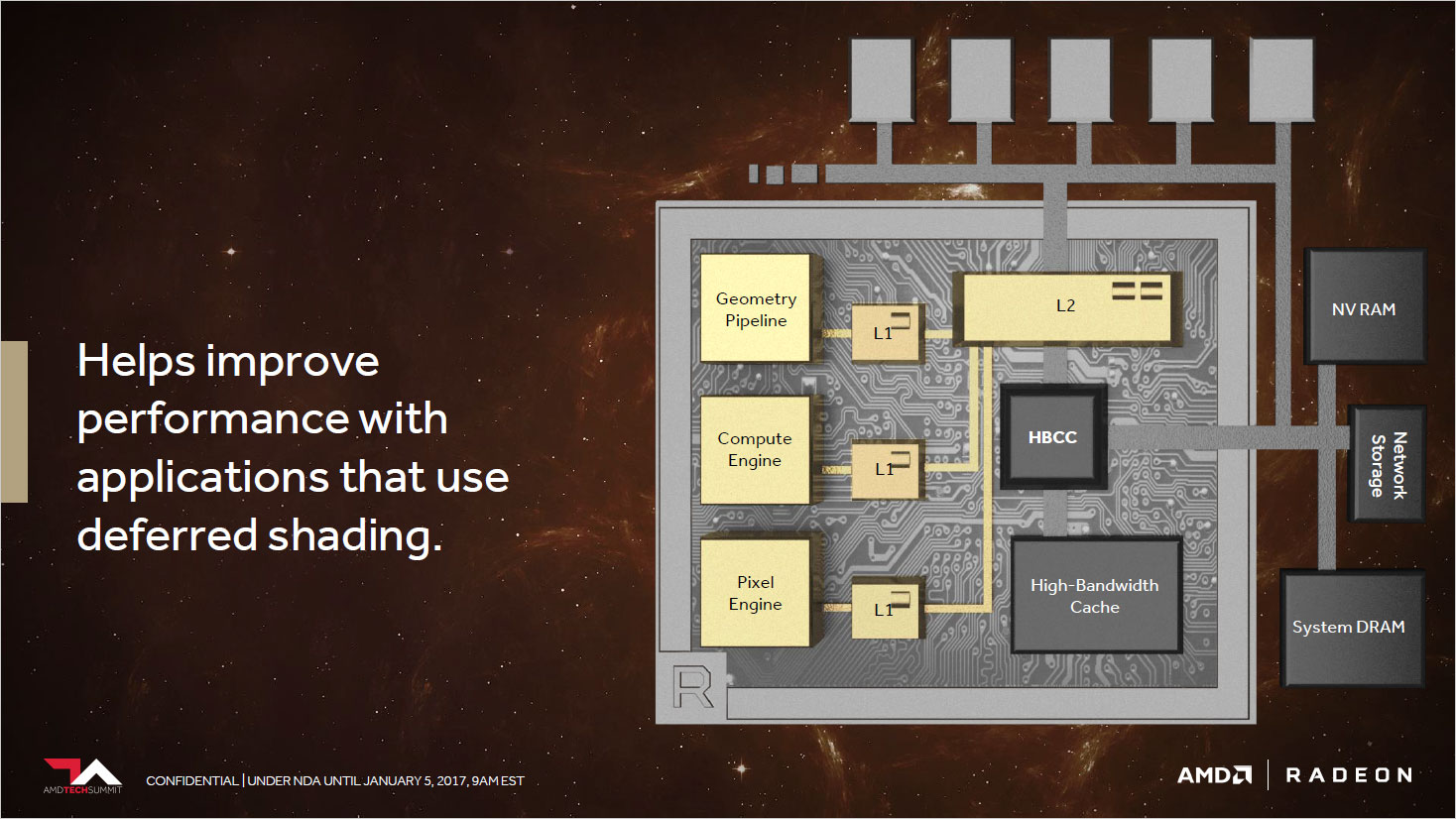
Finally, AMD improved the pixel engine, with a new Draw Stream Binning Rasterizer that helps cull pixels that aren't visible in the final scene. All the render back-ends are also clients of the cache now, reducing the number of memory accesses (e.g., for when the pixel and shader pipelines both access the same texture). This should provide significant performance improvements with deferred rendering engines, which is what many modern games are using.
Based purely on the raw performance numbers, Vega would be impressive, but factor in the other changes and AMD's currently superior DX12/Vulkan performance, and we're looking at another exciting year in graphics cards. The GTX 1080 leads the Fury X by around 30 percent on average (less at 4K), so a 45 percent boost would put Vega well ahead, and if the architecture improvements can add another 10-15 percent Vega might even match or exceed Titan X. AMD has already demoed Doom running at 4K ultra and 65-75 fps (on a Ryzen system, no less), backing up that performance estimate.
For graphics junkies like me, June can't come soon enough.
Here's the complete Vega slide deck from AMD:




Jarred's love of computers dates back to the dark ages when his dad brought home a DOS 2.3 PC and he left his C-64 behind. He eventually built his first custom PC in 1990 with a 286 12MHz, only to discover it was already woefully outdated when Wing Commander was released a few months later. He holds a BS in Computer Science from Brigham Young University and has been working as a tech journalist since 2004, writing for AnandTech, Maximum PC, and PC Gamer. From the first S3 Virge '3D decelerators' to today's GPUs, Jarred keeps up with all the latest graphics trends and is the one to ask about game performance.


